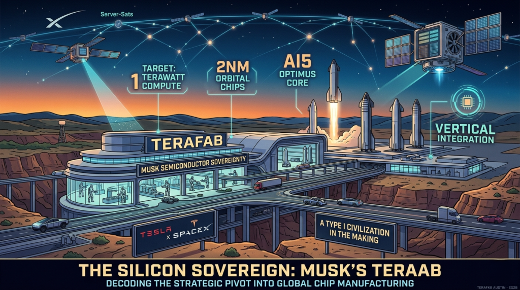
The date March 22, 2026, will likely be remembered as the day the semiconductor industry shifted on its axis. Standing before a crowd of engineers and investors in Austin, Texas, Elon Musk unveiled a roadmap that many had whispered about but few believed would materialize so soon: Elon Musk chip manufacturing is no longer a localized Tesla project—it is a global, multi-industrial mission encompassing SpaceX, Tesla, and xAI.
By announcing the “Terafab,” a massive joint venture designed to produce high-end, AI-optimized silicon at a scale never before seen in the private sector, Musk is effectively declaring independence from the traditional foundry model. This isn’t just about avoiding supply chain hiccups; it’s about the vertical integration of intelligence itself.
The Genesis of the Terafab: Why Now?
To understand the magnitude of Elon Musk chip manufacturing, one must first look at the current bottlenecks facing the “Muskonomy.” Tesla is currently data-rich but compute-constrained. SpaceX requires radiation-hardened processors that can handle the massive telemetry of Starship and the growing Starlink constellation. xAI, the newest pillar of this empire, is hungry for H100-class performance to fuel its Grok models.
Relying on external partners like TSMC or Nvidia, while successful in the short term, introduces a “tax” on innovation. By moving Elon Musk chip manufacturing in-house, these companies can bypass the 18-month lead times and the generic architecture of off-the-shelf components.
The Three Pillars of the Terafab
- AI-First Architecture: Unlike traditional foundries that build for a thousand different customers, the Terafab is optimized for the specific transformer-based architectures used by Tesla FSD and xAI.
- Radiation-Hardened Innovation: SpaceX’s involvement brings a unique requirement: chips that can survive the vacuum of space and high-energy cosmic rays.
- Scale and Sustainability: Musk aims to power these facilities using dedicated Tesla Megapack installations and Starshield-integrated security.
Tesla’s AI5 and the Evolution of the “Inference Engine”
At the heart of the Elon Musk chip manufacturing announcement was the reveal of the AI5 and AI6 processors. While the current Dojo and HW4 systems are industry leaders, the AI5 is designed to be the definitive “brain” for the Optimus humanoid robot.
The Technical Leap
The AI5 isn’t just a bump in FLOPS (floating-point operations per second). It represents a fundamental shift in how power is managed at the edge.
- Power Efficiency: Reducing the wattage required for real-time vision processing by 40%.
- On-Die Memory: Increasing the bandwidth between the neural processing unit (NPU) and the memory to eliminate the “von Neumann bottleneck.”
- Thermal Management: Integrated liquid-cooling pathways directly on the silicon substrate.
By mastering Elon Musk chip manufacturing, Tesla can produce these chips at a fraction of the cost of buying equivalent hardware from third parties, potentially adding billions to Tesla’s bottom line as they scale the Optimus robot production lines.
SpaceX and the Orbital Compute Revolution
Perhaps the most “sci-fi” aspect of the TechCrunch report involves SpaceX’s role in Elon Musk chip manufacturing. Musk envisions a future where “compute is a utility,” much like electricity or water. To achieve this, SpaceX is designing “Server-Sats”—Starlink satellites that are essentially flying data centers.
Why Space-Based Chips?
- Passive Cooling: In the deep cold of space, the heat generated by massive AI training can be dissipated more effectively through specialized radiator fins.
- Global Low Latency: By processing data in orbit rather than sending it to a terrestrial server and back, SpaceX can offer near-instantaneous AI feedback to any point on Earth.
- Energy Sovereignty: These orbital data centers are powered by 24/7 solar energy, unaffected by the Earth’s day/night cycle or atmospheric interference.
The Terafab will be the primary source for these orbital chips, ensuring that Elon Musk chip manufacturing stays ahead of the burgeoning “space-race for silicon” being initiated by rival nations.
Comparing the Giants: Terafab vs. The Industry
To appreciate the audacity of this move, we must compare the proposed Elon Musk chip manufacturing capacity with the current titans of the industry.
| Feature | TSMC (Taiwan Semiconductor) | The Terafab (Musk Vision) |
| Business Model | Foundry for hire (Nvidia, Apple, etc.) | Fully Vertical (Internal consumption) |
| Node Tech | 2nm and 3nm Leading Edge | 2nm optimized for AI Inference |
| Supply Chain | Global, fragmented | Localized (Texas/Nevada/Space) |
| Annual Capacity | ~15 million wafers | ~5 million (Targeting 15% of global high-end) |
| Focus | General Purpose / Mobile | Neural Networks / Robotics / Space |
The comparison shows that while Musk isn’t trying to replace the entire semiconductor industry, Elon Musk chip manufacturing is designed to capture the most valuable segment: high-performance AI and robotics.
The Economic Ripple Effects of In-House Silicon
When a company as large as Tesla or SpaceX stops buying chips and starts making them, the market feels the tremors. Elon Musk chip manufacturing creates a “moat” that is nearly impossible for competitors like Ford, GM, or Blue Origin to cross.
1. Cost Reduction at Scale
By removing the profit margin of the middleman (the foundry), the cost per unit for a Tesla vehicle’s computer could drop by as much as 30%. This allows Musk to further lower the price of EVs while maintaining high margins.
2. Rapid Iteration
In the current model, if Tesla wants to change a chip design, they have to wait for the next fabrication cycle at an external foundry. With Elon Musk chip manufacturing, the “design-to-dirt” time is slashed. Engineers can test a new architecture on Monday and have prototype silicon in a test vehicle within weeks.
3. Talent Magnetism
The Terafab will require the world’s best lithography experts and material scientists. This move positions Musk’s companies at the center of the “Silicon Renaissance,” drawing talent away from traditional hubs like Silicon Valley and into the “Silicon Hills” of Austin.
Overcoming the Challenges of High-End Fabrication
It would be a mistake to assume that Elon Musk chip manufacturing will be without its “production hell.” Semiconductor fabrication is arguably the most complex manufacturing process on the planet.
“Making chips is easy. Making millions of chips with a 99% yield is a nightmare,” Musk admitted during the presentation.
The Lithography Hurdle
To reach the 2nm node, Musk will need EUV (Extreme Ultraviolet) lithography machines, currently only produced by ASML in the Netherlands. Securing these machines is a geopolitical challenge as much as a financial one. However, the report suggests that Elon Musk chip manufacturing may be exploring alternative, proprietary lithography techniques to reduce reliance on external hardware.
The Talent Gap
Building a “fab” requires thousands of specialized technicians. Musk plans to address this through the “Tesla U” initiative, a vocational training program designed to pipeline students directly into the Elon Musk chip manufacturing workforce.
Actionable Strategy: What Should Investors and Tech Leaders Do?
The announcement of Elon Musk chip manufacturing isn’t just news; it’s a signal. Here is how different sectors should respond:
- For Investors: Look beyond the “car company” narrative for Tesla. Tesla is now a robotics and semiconductor company. Evaluate its valuation based on its compute capacity rather than just vehicle deliveries.
- For Tech Competitors: The era of “outsourced intelligence” is ending. Companies that do not own their silicon roadmap will find themselves at a structural disadvantage in the age of AI.
- For Supply Chain Managers: Expect a shift in demand for raw materials like silicon, neon gas, and specialized polymers as Elon Musk chip manufacturing ramps up its terrestrial footprint.
The Future: A Silicon-Powered Civilization
Musk’s vision for Elon Musk chip manufacturing extends far beyond the next quarterly report. He is building the foundation for what he calls a “Type I Civilization”—one that can harness the full energy and informational potential of its home planet and surrounding orbit.
The Terafab is the engine of this transition. By controlling the silicon, Musk controls the speed of AI development, the efficiency of autonomous transport, and the reach of human communication. Elon Musk chip manufacturing is the final piece of the puzzle that connects the ground, the robot, and the stars.
Key Takeaways from the Unveiling:
- Vertical Integration is King: Controlling the chip is the only way to ensure the software’s peak performance.
- Space is the New Frontier for Compute: Expect “Server-Sats” to become a major part of the SpaceX business model.
- The AI5/AI6 Chips: These will be the most advanced edge-AI processors in the world, specifically tuned for the Optimus robot.
- A $25 Billion Bet: This is one of the largest capital expenditures in Musk’s history, signaling total confidence in the future of AI.
Conclusion: The New Era of Tech Sovereignty
As we look toward the late 2020s, the move into Elon Musk chip manufacturing stands as a testament to the power of bold, long-term thinking. While the rest of the world worries about chip shortages, Musk is building a factory to end them—at least for himself.
The Terafab isn’t just a building; it’s a manifesto. It says that the future belongs to those who build the hardware that runs the world. With Elon Musk chip manufacturing now in full swing, the race to define that future has officially begun.
The Geopolitical Chessboard: Silicon as the New Oil
The shift toward Elon Musk chip manufacturing isn’t just a corporate strategy; it is a geopolitical maneuver. For decades, the world has been dangerously reliant on a handful of square miles in Taiwan for the world’s most advanced logic chips. By establishing the Terafab in the United States and extending compute capabilities into orbit, Musk is effectively “de-risking” the future of AI from terrestrial conflicts.
This “Silicon Sovereignty” ensures that if a global supply chain collapse occurs, the progress of Full Self-Driving and the deployment of Optimus will not grind to a halt. In this new era, the wealth of a company—or a nation—will not be measured by its gold reserves, but by its flops-per-watt and its ability to manufacture the “brains” that power autonomous systems.
Environmental Paradox: Is Mass Fabrication Sustainable?
One of the most frequent critiques of Elon Musk chip manufacturing is the environmental toll. Traditional semiconductor fabs are notorious for their massive water consumption and carbon footprint. However, Musk’s approach seeks to invert this narrative. By integrating Tesla’s solar and battery storage technology directly into the fab’s infrastructure, the Terafab aims to be the first “net-zero” high-volume semiconductor facility.
Furthermore, by moving high-heat AI training workloads to orbital “Server-Sats,” Musk is addressing the growing energy crisis on Earth’s power grids. Space provides an infinite heat sink and 24/7 solar exposure, potentially making Elon Musk chip manufacturing and the resulting compute cycles the most energy-efficient in human history.
The “Master Plan” Conclusion: Closing the Loop
When Elon Musk released his first “Master Plan” nearly two decades ago, many saw a car company. With the announcement of the Terafab, the final layer of the Master Plan is revealed: The unification of energy, transport, and intelligence.
We are moving into a decade where the distinction between a software company and a hardware company disappears. Elon Musk chip manufacturing is the glue that holds this vision together. From the silicon wafers in Austin to the orbiting processors in the night sky, the goal remains the same—to accelerate the transition to a world where intelligence is as abundant and accessible as the air we breathe.
Whether you view this as a bold leap for humanity or a risky overextension of resources, one thing is certain: the semiconductor industry will never be the same. The Terafab is officially open for business, and the “Silicon Hills” of Texas are now the epicenter of the next industrial revolution.
Frequently Asked Questions (FAQ)
To provide further clarity on the monumental shift in Elon Musk chip manufacturing, we have compiled the most pressing questions from the tech community and investors following the March 2026 announcement.
1. What is the Terafab, and where is it located?
The Terafab is a $25 billion joint venture between Tesla, SpaceX, and xAI. It is the world’s first fully vertically integrated semiconductor fabrication facility, handling everything from chip design and lithography to final testing under one roof. The facility is currently under construction at the North Campus of Giga Texas in Austin, occupying an estimated 5 million square feet of new building space.(How Elon Musk builds chips)
2. Why is Elon Musk moving into chip manufacturing now?
According to Musk, the move is “existential.” Existing suppliers like TSMC, Samsung, and Micron have a maximum expansion rate that cannot keep pace with the exponential compute needs of the Optimus robot and Tesla’s FSD (Full Self-Driving) fleet. Musk stated, “We either build the Terafab, or we don’t have the chips.”
3. What are the specific chips being produced?
The facility is focused on two primary silicon categories:
- Inference Chips (AI5 & AI6): Optimized for low-latency edge computing in Tesla vehicles and Optimus humanoid robots. These are designed to be 40x–50x more performant than the previous AI4 hardware.
- Space-Grade Chips (D3): Radiation-hardened and high-temperature-resistant processors designed specifically for SpaceX’s orbital data centers.
4. How does the Terafab compare to TSMC?
While TSMC remains the global leader, the Terafab aims for a staggering output of 1 million wafer starts per month at the 2-nanometer (2nm) node. For context, this would represent roughly 70% of TSMC’s current global capacity—all centralized in a single Austin location.
5. What is the “Orbital Compute” plan mentioned in the report?
SpaceX has filed with the FCC to deploy up to one million “Server-Sats.” These are satellites that function as orbital data centers. By leveraging the vacuum of space for cooling and 24/7 solar irradiance, Musk believes orbital AI compute will become significantly cheaper than terrestrial alternatives within the next 2-3 years.
6. Will these chips be available for other companies to buy?
Initially, no. 100% of the Terafab’s output is earmarked for internal use across the “Muskonomy.” However, during the March 21 presentation, Musk hinted that once internal demand is met, the excess capacity could eventually be offered as a cloud-compute service (likely via xAI).
7. How is the Terafab being funded?
The project is estimated to cost between $20 billion and $25 billion. Interestingly, Tesla’s CFO clarified that this expenditure was not yet part of the standard 2026 CAPEX plan, suggesting it may be funded through a combination of SpaceX private equity, a potential SpaceX IPO, and xAI investment rounds.(SpaceX Terafab Austin)
8. What are the biggest risks to the project?
The three primary hurdles are:
- Technical Complexity: Leading-edge 2nm fabrication is notoriously difficult to yield at high volumes.
- Talent Acquisition: Finding enough specialized lithography and material science engineers to staff a facility of this scale.
- Resource Constraints: Global shortages of neon and helium—essential for chipmaking—could delay the operational timeline.
Final Thoughts: The Road to 2030
The move toward Elon Musk chip manufacturing is the final piece of a decade-long puzzle. By owning the silicon, Musk is no longer just a participant in the AI revolution; he is the architect of its physical foundation. Whether it’s a robot in your home or a server in the stars, the “Silicon Sovereignty” of the Terafab ensures that the future of intelligence stays firmly within the Musk ecosystem.(Tesla AI5 processor)