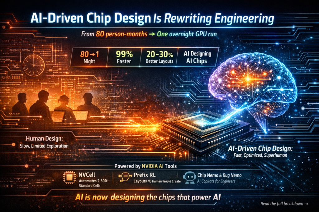
NVIDIA just compressed 80 person-months of chip design work into a single overnight GPU run — and the AI-generated results are better than what human engineers produced. This is not a future projection; it is already happening inside one of the world’s most advanced semiconductor companies, and it signals a fundamental shift in how silicon gets built.
AI-driven chip design is no longer a research curiosity. It is a production reality that is compressing timelines, cutting costs, and — in some cases — producing circuit layouts that no human engineer would have conceived. Here is everything you need to know about what NVIDIA has built, how it works, and why it matters for the future of computing. (AI-driven chip design, reinforcement learning chip design, NVIDIA NVCell, semiconductor automation, AI EDA tools)
What Is AI-Driven Chip Design?
Definition: AI-driven chip design refers to the use of machine learning models — particularly reinforcement learning and large language models — to automate, accelerate, or optimize stages of the semiconductor design process that have traditionally required large teams of expert engineers working over months or years.
Expansion: Modern chips contain billions of transistors organized into thousands of functional cells. Designing, verifying, and porting those cells across new manufacturing processes involves enormous combinatorial complexity. Traditional electronic design automation (EDA) tools help, but they still rely heavily on human expertise to navigate the design space. AI-driven chip design replaces or augments that human effort with systems that can explore millions of configurations autonomously, often arriving at solutions that outperform hand-crafted designs on metrics like power, area, and timing delay. (AI-driven chip design, reinforcement learning chip design, NVIDIA NVCell, semiconductor automation, AI EDA tools)
NVIDIA’s Breakthrough — From 80 Person-Months to One Night
At NVIDIA’s GTC 2026 conference, Chief Scientist Bill Dally revealed the clearest public evidence yet of how AI-driven chip design is transforming internal engineering workflows. Speaking with Google Chief Scientist Jeff Dean, Dally described how porting NVIDIA’s standard cell library to a new semiconductor process used to require a team of eight people working for roughly ten months — 80 person-months in total. A reinforcement learning-based tool called NVCell now completes that same work overnight on a single GPU, with results that can match or exceed human designs across measures of size, power dissipation, and delay. VideoCardz
That single data point deserves to be held up and examined carefully. Eighty person-months is approximately 6.7 years of a single engineer’s full-time effort. Compressing that into one overnight compute job does not just save money — it removes a major bottleneck that has historically slowed NVIDIA’s ability to adopt new chip manufacturing processes from TSMC and other foundries.
Dally framed the impact bluntly: it eliminates an obstacle to moving to new processes, because standard cell libraries can now be ported very quickly. VideoCardz In an industry where every process node transition represents a potential 12–24 month delay, that is a strategic advantage of enormous magnitude.
The Tools Behind the Transformation
NVIDIA is not relying on a single AI system. The company is applying AI across design exploration, standard cell library work, bug handling, and verification — multiple distinct stages of the chip development pipeline. VideoCardz Three internal tools illustrate how deep this integration has gone.
NVCell — Automating Standard Cell Libraries
NVCell is NVIDIA’s reinforcement learning-based tool for porting standard cell libraries to new process nodes. Each library contains roughly 2,500 to 3,000 individual cells. What once took eight engineers about ten months now runs overnight on one GPU, producing results that are actually better than human designs in terms of cell size, power consumption, and timing delay. PC Gamer
Standard cells are the foundational building blocks of digital chip design — think of them as the alphabet from which every circuit is written. Getting them right for each new semiconductor process is painstaking work. NVCell turns that painstaking work into an automated overnight computation, representing one of the most concrete wins for AI-driven chip design published to date.
Prefix RL — Superhuman Circuit Layouts
Beyond cell libraries, NVIDIA has developed a tool called prefix RL that targets the long-studied problem of placing look-ahead stages in a carry lookahead chain. The system produces layouts that “no human would ever come up with,” while improving key metrics by roughly 20 to 30% compared to human designs. VideoCardz
This is a qualitatively different kind of result. NVCell is faster than humans; prefix RL is finding solutions in a part of the design space that human engineers systematically miss. Reinforcement learning chip design, when applied to problems humans have studied for decades, is not just automating the known path — it is discovering new paths entirely.
Chip Nemo & Bug Nemo — AI for Engineering Teams
NVIDIA also runs internal large language models called Chip Nemo and Bug Nemo, fine-tuned on proprietary NVIDIA material including RTL and architecture documents for GPUs designed over the years. Junior engineers can query these models instead of repeatedly consulting senior designers about how a specific block works, while Bug Nemo can summarize bug reports and help route them to the right module or engineer. VideoCardz
This is a subtler but equally important form of AI-driven chip design. The knowledge embedded in years of GPU architecture documents is not lost when senior engineers rotate or retire — it is encoded into a queryable model that accelerates onboarding, reduces interruptions for experienced staff, and shortens the time between identifying a bug and fixing it.
By the Numbers — Human vs. AI Chip Design
The following table summarizes the performance differences NVIDIA has reported between traditional human-led chip design workflows and their AI-driven equivalents:
| Design Task | Traditional Approach | AI-Driven Approach | Improvement |
|---|---|---|---|
| Standard cell library porting (NVCell) | 8 engineers × 10 months = 80 person-months | Overnight on 1 GPU | ~99%+ time reduction |
| Cell quality (size, power, delay) | Human baseline | Matches or exceeds human | Equal or better |
| Carry lookahead chain placement (Prefix RL) | Expert human design | RL-generated layout | 20–30% better on key metrics |
| Bug triage & routing (Bug Nemo) | Senior engineer judgment | LLM-assisted routing | Faster, scalable |
| Junior engineer onboarding | Direct consultation with seniors | Query Chip Nemo | Reduced interruptions |
The pattern that emerges is consistent: AI-driven chip design is not selectively better in one corner of the workflow. It is producing gains across multiple stages, from physical cell layout to software-layer debugging.
How Reinforcement Learning Makes This Possible
What is reinforcement learning in chip design? Reinforcement learning (RL) is a machine learning paradigm in which an agent learns to make decisions by taking actions, observing the outcomes, and adjusting its strategy to maximize a reward signal. In chip design, the “actions” are design choices — where to place a circuit element, how to size a cell, how to route a signal — and the “reward” is a combination of physical metrics like area, power, and timing.
Why does RL work especially well here? Chip design is a combinatorial optimization problem of staggering scale. A standard cell library with 3,000 cells, each with dozens of tunable parameters, creates a search space that exhaustive human analysis cannot fully explore. RL agents do not get fatigued, do not rely on prior heuristics that may be suboptimal, and can run millions of trial configurations in the time it takes a human team to review a handful. This is precisely why reinforcement learning chip design produces layouts that, as Dally put it, no human would ever come up with — the AI is exploring regions of the design space that human intuition never led engineers toward.
What This Means for the Semiconductor Industry
The implications of AI-driven chip design extend well beyond NVIDIA’s internal productivity metrics.
Faster process node adoption. Every new semiconductor process node — from 7nm to 5nm to 3nm — requires expensive, time-consuming re-engineering of design libraries and tools. If AI can collapse that re-engineering timeline from months to days, chipmakers gain the ability to move faster between nodes. This accelerates the performance curve of computing hardware broadly.
Lower barriers to chip design. The expertise required to design a competitive standard cell library has historically been concentrated in a small number of elite engineering teams at companies like NVIDIA, Intel, and TSMC. AI-driven chip design tools democratize access to that expertise, potentially enabling smaller semiconductor companies and startups to compete at a higher level.
Changing engineering roles. NVIDIA has been careful to characterize AI as a design tool rather than a design authority — engineers remain involved, assessing the results of overnight runs and making the ultimate decisions. Fortune Herald The role of the chip engineer is shifting from performing optimization manually to curating and validating AI-generated design candidates. This is not the elimination of engineering judgment; it is the elevation of it.
Competitive moat. For NVIDIA specifically, the internal mastery of AI-driven chip design creates a compounding advantage. Each generation of chips can be designed faster and at higher quality, which means each generation of AI hardware is more competitive — which in turn generates the computational resources needed to run better AI design tools in the next cycle.
The Recursive Loop — AI Designing Better AI Chips
There is something philosophically striking about NVIDIA’s situation that deserves explicit acknowledgment. NVIDIA not only produces the chips that AI systems use — it uses those very AI systems to build the next generation of processors. With each hardware generation feeding the design of the next, the loop is closing on itself. Fortune Herald
Jensen Huang has stated publicly that NVIDIA can no longer build semiconductors or write software without this AI-driven approach — not “could benefit from,” but no longer able to. Fortune Herald That framing is significant. It suggests that the design complexity of modern chip architecture has already surpassed what human cognitive capacity alone can manage fully. AI is not augmenting chip design at the margins — it has become structurally necessary to it.
This recursive dynamic — AI-designed chips powering better AI tools that design even better chips — is what makes the current moment a genuine inflection point, not merely an incremental efficiency gain.
Is Fully Automated Chip Design on the Horizon?
Question: Will AI replace human chip designers entirely?
Direct answer: Not soon, and possibly never in a complete sense — but the boundary is moving faster than most observers expected.
Bill Dally was direct at GTC 2026: fully end-to-end automated chip design is still far off. VideoCardz The current state of AI-driven chip design is one of targeted automation — specific sub-tasks like cell library porting, carry chain optimization, and bug triage have been successfully automated, while other stages of chip design (architecture decisions, system-level tradeoffs, manufacturability sign-off) remain deeply human-driven.
The more nuanced question is not whether full automation is coming, but whether the boundary will continue to shift. Five years ago, automating an 80-person-month cell library task overnight on a single GPU would have seemed implausible. The fact that it is a production reality today suggests that predictions about AI design automation should be held loosely.
What seems likely is a continued expansion of the domains where AI-driven chip design outperforms human-only approaches, with human engineers progressively moving up the abstraction stack — focusing on architectural strategy and verification while AI handles the combinatorial optimization beneath.
Key Takeaways
- AI-driven chip design has moved from research to production, with NVIDIA using it across multiple internal workflows including cell library creation, circuit placement, bug triage, and design verification.
- NVCell, NVIDIA’s reinforcement learning chip design tool, compressed an 80-person-month standard cell library porting task into a single overnight GPU run — with better results than human engineers.
- Prefix RL goes further, generating carry lookahead chain layouts that improve on human designs by 20–30% in key metrics and that human engineers would never have discovered independently.
- Chip Nemo and Bug Nemo encode decades of GPU architecture knowledge into queryable LLMs, accelerating junior engineer development and bug resolution.
- The semiconductor industry is entering a period where AI EDA tools and reinforcement learning chip design are not optional productivity boosters but structural requirements for competitive chip development.
- The recursive loop — AI chips enabling better AI design tools enabling better AI chips — represents a compounding dynamic that will shape the trajectory of computing hardware for years to come.
Further Reading:
- NVIDIA GTC 2026: Bill Dally and Jeff Dean, “Advancing to AI’s Next Frontier”
- NVIDIA Technical Blog: Inside the Blackwell Ultra Architecture
- PC Gamer: How NVIDIA Uses AI to Design Its Next-Generation GPUs
❓ Frequently Asked Questions (FAQ)
1. What is AI-driven chip design and why is it important?
AI-driven chip design refers to the use of artificial intelligence techniques, especially machine learning and reinforcement learning, to automate and optimize the semiconductor design process. Traditionally, chip design has required months or even years of manual work by highly skilled engineers. AI changes this by enabling systems to explore millions of design possibilities much faster than humans can.
The importance of this shift lies in speed, efficiency, and innovation. As chips become more complex with billions of transistors, human-driven approaches struggle to keep up. AI not only accelerates the process but also discovers design patterns that humans might overlook. This leads to better performance, lower power consumption, and more efficient use of space on a chip, making it a critical advancement for the future of computing.
2. How does reinforcement learning improve chip design?
Reinforcement learning improves chip design by treating it as an optimization problem where an AI agent learns through trial and error. The system makes design decisions—such as component placement or routing—and receives feedback based on performance metrics like power, area, and speed.
Over time, the AI learns which decisions lead to better outcomes and refines its strategy. Unlike human engineers who rely on experience and heuristics, reinforcement learning can test a vast number of configurations quickly. This allows it to identify highly optimized solutions, including unconventional layouts that humans may never consider. As a result, reinforcement learning significantly enhances both the efficiency and quality of chip designs.
3. What is NVIDIA’s NVCell tool and how does it work?
NVCell is an AI-powered tool developed to automate the creation and porting of standard cell libraries, which are essential building blocks in chip design. These libraries contain thousands of pre-designed logic components used to construct complex circuits.
Previously, porting these libraries to a new manufacturing process required months of effort from a team of engineers. NVCell uses reinforcement learning to automate this process, generating optimized designs in a fraction of the time. It evaluates different configurations based on key metrics like power usage, size, and timing delay, and iteratively improves the design.
The result is not only faster production but also higher-quality outputs, making NVCell a powerful example of how AI is transforming semiconductor workflows.
4. Can AI fully replace human chip designers?
AI is unlikely to completely replace human chip designers in the near future. While AI excels at handling repetitive, complex optimization tasks, human engineers are still essential for high-level decision-making, architectural planning, and ensuring that designs meet real-world requirements.
Instead of replacement, the industry is moving toward collaboration. AI acts as a powerful tool that augments human capabilities, allowing engineers to focus on strategy and innovation rather than manual optimization. This shift enhances productivity and enables teams to tackle more ambitious projects.
In essence, AI is changing the role of chip designers rather than eliminating it, making them more efficient and impactful.
5. What are the main benefits of AI in semiconductor design?
The integration of AI into semiconductor design brings several key benefits. First, it dramatically reduces design time, turning processes that once took months into tasks that can be completed in hours or days. This acceleration helps companies bring products to market faster.
Second, AI improves design quality by exploring a larger solution space and identifying more efficient configurations. This results in chips that are smaller, faster, and more energy-efficient. Third, it reduces dependency on large engineering teams, lowering costs and making advanced chip design more accessible.
Finally, AI enables continuous improvement. As models learn from past designs, they become better over time, creating a compounding advantage for organizations that adopt these technologies early.
6. What does the future of AI-driven chip design look like?
The future of chip design is increasingly automated and intelligent. As AI tools continue to evolve, they will take on more responsibilities across the design pipeline, from layout optimization to verification and debugging. This will further reduce development cycles and improve overall chip performance.
One of the most exciting trends is the idea of AI designing chips that are specifically optimized for running AI workloads. This creates a feedback loop where better chips enable more advanced AI, which in turn designs even better chips.
While full automation may still be years away, the direction is clear: AI will play a central role in shaping the next generation of semiconductor innovation, making the design process faster, smarter, and more scalable than ever before.