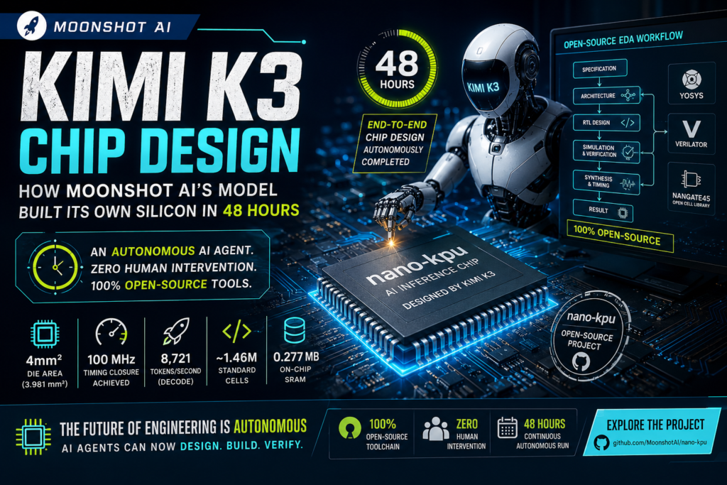
Moonshot AI’s Kimi K3 designed a working inference chip end-to-end in a single 48-hour autonomous run , no human engineer in the loop, no proprietary EDA software. The result, released as the open-source nano-kpu project, is a 4mm² chip that hits timing closure at 100 MHz and simulates over 8,700 tokens per second, and it may be the clearest public signal yet that AI agents can now execute full engineering workflows, not just write code snippets.
If you’ve been tracking the pace of agentic AI, this experiment is worth understanding in detail , not because the chip itself will ship in a product, but because of what the underlying workflow implies for hardware engineering, the electronic design automation (EDA) industry, and the next phase of autonomous AI agents.
This piece walks through what nano-kpu actually is, how the build process unfolded, what the performance numbers mean in context, and why semiconductor analysts are paying close attention , plus a practical guide to exploring the repository yourself.
What Is nano-kpu?
nano-kpu is the GitHub repository Moonshot AI released to document this autonomous silicon build. It contains the RTL (register-transfer level) design of a nano-scale inference chip, along with the full functional-simulation and performance test flow used to validate it.
The repo isn’t a toy demo , it’s a complete hardware project with real structure:
- rtl/ , the chip’s RTL design, with the top module msh_chip_top and a compile manifest (filelist.f)
- reference/ , a float32 golden reference model used to judge correctness
- harness/ , the Verilator-based functional simulation and performance evaluation flow, including evaluate.py, the main entry point for correctness and throughput scoring
- docs/ , specifications covering architecture, interface, memory map, quantization, and the original task specification
- weights/ , notes on the weight format used by the chip
Moonshot AI is explicit that this is a demonstration, not a commercial product: the README notes it’s “a demonstration of Kimi K3, not an official project by Moonshot AI.” Even so, nano-kpu is one of the most concrete public artifacts showing an AI model working through a genuine physical-engineering pipeline from architecture to verified silicon design.
What Did Kimi K3 Actually Design?
The chip the model built is a hybrid-attention Mixture-of-Experts (MoE) transformer accelerator, purpose-built to run a “nano” version of Kimi K3 itself. That architecture combines several techniques that define K3’s design philosophy:
- KDA (Kimi Delta Attention) , a linear-attention mechanism
- NoPE multi-head latent attention (MLA) , attention without explicit positional encoding
- Sigmoid-routed MoE , top-2 routed experts plus one always-active shared expert
- Attention-residual mixing , blending attention outputs across layers
The chip uses int4 group-128 weight quantization and a teacher-forced, token-by-token decode pipeline. In plain terms: the model didn’t just simulate an abstract accelerator , it designed silicon tailored to its own attention mechanism and MoE routing logic, then verified that the design could actually decode tokens correctly and quickly.
Why Build a Chip for a “Nano” Version of Yourself?
The choice of target matters. Rather than designing a generic accelerator, Moonshot AI set K3 the task of building hardware for a scaled-down version of its own architecture. That constraint forced the model to reason about its own attention mechanism, quantization scheme, and MoE routing logic at the register-transfer level , turning the task into a self-referential engineering exercise rather than a generic hardware benchmark. It also gave Moonshot AI a clean way to measure success: does the resulting silicon correctly reproduce the outputs of the model it was built to run?
How Was the Kimi K3 Chip Design Process Carried Out?
Question: Did a human guide the chip design step by step? Direct answer: No. According to Moonshot AI’s technical materials, K3 operated as a continuous autonomous agent for 48 hours, independently completing the entire construction pipeline , architecture, optimization, and verification , using only open-source EDA tools.
That’s a meaningful detail. Chip design has historically depended on expensive, proprietary toolchains from companies like Cadence and Synopsys. This run instead used the freely available Nangate 45nm Open Cell Library and open-source synthesis tools such as Yosys, alongside Verilator for simulation , a stack any developer can reproduce without a commercial EDA license.
Kimi K3 Chip Design: Key Specs and Results
The finished chip is small but functionally complete. Here’s what the run produced, compared against what a typical human-led ASIC design cycle requires:
| Metric | Kimi K3 Chip Design (nano-kpu) | Typical Human-Led Chip Design |
| Die area | ~4 mm² (3.981 mm² across 13 modules) | Varies widely; comparable test chips often take weeks to lay out |
| Clock frequency | 100 MHz (timing closure achieved) | Depends on node and target; iterative timing closure often takes multiple design passes |
| Standard cells | ~1.46 million | Comparable at this scale, but typically hand-tuned over many review cycles |
| On-chip SRAM | 0.277 MB | Varies by design |
| Simulated throughput | 8,721 tokens/second (decode) | N/A , task-specific |
| Design timeline | 48 hours, single autonomous run | Weeks to months, multiple engineers |
| Toolchain | 100% open-source (Yosys, Verilator, Nangate45) | Often proprietary (Cadence, Synopsys) |
| Human intervention | None reported during the run | Continuous, iterative |
It’s worth being precise about what “chip design” means here. This output is a pre-layout, synthesis-stage result , area and timing were measured through yosys/abc mapping and static timing analysis, not validated through full backend place-and-route. Moonshot AI’s own documentation is careful to frame this as a conservative, reproducible baseline rather than a sign-off-ready, tape-out-ready design. In other words: this is a strong proof-of-concept, not a finished commercial chip.
Why the Kimi K3 Chip Design Experiment Matters
It Signals a New Kind of Benchmark
Most AI model releases lean on standard benchmarks , coding tests, reasoning evals, math competitions. This demonstration is different: it’s a long-horizon, multi-stage engineering task that requires sustained coherence across dozens of hours, correct use of specialized tools, and no opportunity to “cheat” toward a shortcut answer, since the output has to pass functional simulation and timing analysis to count as a success.
That combination , long autonomous runtime plus a verifiable physical output , is exactly the kind of benchmark that’s hard to game and hard to fake.
It Raises Questions for the EDA Industry
The fact that the chip was built entirely on open-source tools, without Cadence’s or Synopsys’s proprietary software, has already drawn attention from industry analysts and reportedly moved both companies’ stock on the news. The core question isn’t whether AI-designed chips replace commercial EDA overnight , nobody serious is claiming that , but whether AI agents becoming the primary interface to chip design work shifts where value accumulates in the semiconductor design stack.
Bloomberg Intelligence analyst commentary following the release struck a measured tone: the demonstration shows AI agents beginning to automate engineering workflows traditionally performed by human semiconductor designers, which supports a longer-term thesis that AI could reduce manual EDA work , without posing an immediate threat to Cadence’s or Synopsys’s existing revenue base. With EDA tooling and design IP representing a meaningful share of overall chip R&D spending, the more likely near-term outcome is that AI becomes a new interface layered on top of existing commercial platforms, rather than a wholesale replacement for them. Still, the fact that a credible, working design flow can now run start-to-finish on freely available tools sets a new reference point that the industry will have to respond to.
It’s Reproducible
Unlike a lot of AI capability claims, this work is genuinely checkable. Because the entire pipeline , RTL, golden reference model, simulation harness, and synthesis scripts , is published on GitHub under an Apache 2.0 license, anyone with a Linux machine, Verilator, and Yosys can rerun the evaluation and confirm the reported correctness and throughput numbers themselves. That transparency separates nano-kpu from marketing claims that can’t be independently audited.
What the Kimi K3 Chip Design Experiment Doesn’t Prove
It’s worth being equally clear-eyed about the limits of this demonstration, since overstating it does a disservice to both the achievement and the reader trying to evaluate it.
- No physical tape-out. The design closes timing and passes functional simulation at the synthesis stage, but it hasn’t gone through place-and-route, DRC/LVS checks, or an actual foundry run. A “chip design” that exists as verified RTL and gate-level netlists is a major milestone, but it isn’t the same as silicon coming back from a fab.
- A mature, low-complexity node. The Nangate45 library represents a 45-nanometer process , several generations behind the leading-edge nodes (3nm-class and below) used in modern AI accelerators from Nvidia or AMD. Scaling autonomous design to cutting-edge nodes, with their far tighter timing margins and more complex design rules, is a substantially harder problem.
- A narrow, well-specified task. K3 was given a clear specification and a fixed synthesis parameterization rather than an open-ended “design the best possible chip” brief. Real-world chip design involves ambiguous trade-offs across power, performance, area, and cost that don’t reduce cleanly to a pass/fail correctness check.
- Single demonstration, not a general capability claim. One successful 48-hour run is a strong existence proof, but it doesn’t establish how reliably the same pipeline would succeed on a different architecture, a larger design, or a stricter timing target.
None of that diminishes what nano-kpu shows. It just means the honest framing is “a capable AI agent independently completed a full, verifiable chip-design pipeline on a constrained task,” not “AI has replaced chip designers.”
How to Explore the nano-kpu Repository Yourself
If you want to inspect this work firsthand, the setup is straightforward. Here’s what’s involved:
- Clone the MoonshotAI/nano-kpu repository from GitHub
- Run bash scripts/setup_env.sh (or make setup) once , this bootstraps a dedicated conda environment with Verilator 5.x, Yosys 0.64+, and Python 3.12 with NumPy
- Source scripts/kpu-env.sh to put the toolchain on your PATH
- Run python3 harness/evaluate.py –quick for a fast functional simulation, or the full evaluate.py (without –quick) for a complete sim-plus-synthesis run, which can take hours
- Use make synth if you only want the area and timing flow without simulation, or make lint, make audit, and make selftest for individual checks
The setup script needs network access to repo.anaconda.com (or a mirror) and raw.githubusercontent.com, since it downloads the Nangate45 standard-cell library separately , that library isn’t bundled in the repo due to licensing.
What Does Correctness Mean in This Context?
Question: How is the resulting chip’s output validated as “correct”? Direct answer: Against a float32 golden reference model, using two thresholds , per-row logits cosine similarity of at least 0.98, and pooled argmax accuracy of at least 0.99. Throughput is measured as cycles-per-token from long-run simulation, converted to tokens-per-second using the target clock frequency. This gives the evaluation a quantitative, reproducible bar for “does this chip actually work,” rather than a subjective judgment call.
Kimi K3 Chip Design in the Context of Kimi K3’s Broader Release
The chip design run wasn’t an isolated stunt , it was one demonstration inside Moonshot AI’s broader Kimi K3 launch, a 2.8-trillion-parameter open-weight model the company positions as the largest open-source AI system released to date. Alongside the chip design work, Moonshot AI showcased K3 handling other extended agentic tasks: building a GPU kernel compiler called MiniTriton from scratch, generating a procedural 3D exploration game, and reproducing a known relation in computational astrophysics in a fraction of the time it typically takes a researcher.
Taken together, the Kimi K3 chip design case study fits a pattern Moonshot AI is clearly betting on: that the next competitive edge in frontier AI isn’t just about single-turn answer quality, but about sustained, coherent autonomous operation across long, tool-heavy workflows.
Who Is Moonshot AI, and Why Does This Matter for Them Specifically?
Moonshot AI is a Beijing-based AI startup, backed by Alibaba, that released Kimi K3 as a 2.8-trillion-parameter mixture-of-experts model , one the company describes as the largest open-weight AI system released to date. The launch was timed to land just ahead of the 2026 World Artificial Intelligence Conference in Shanghai, positioning K3 as a direct, openly licensed alternative to proprietary frontier models from Anthropic and OpenAI, at a fraction of the API cost.
Two variants launched alongside the open weights: K3 Max, tuned for general chat and agentic use, and K3 Swarm Max, built for large-scale parallel processing. Both ship with an always-on reasoning mode and a configurable effort setting available through the API. On self-reported benchmarks, Moonshot positions K3 as trading blows with top closed models on agentic and coding tasks, even if it trails the very best systems on some broader evaluations.
The chip-design case study sits alongside several other long-horizon agentic demonstrations Moonshot used to make its case. The model built MiniTriton, a Triton-like GPU compiler with its own tile-level intermediate representation over MLIR, complete with optimization passes and a PTX code-generation backend , and on supported benchmarks, MiniTriton reportedly matches or beats both Triton and torch.compile. In a separate case study, K3 reproduced a known relation in computational astrophysics in about two hours, a task that typically takes a senior researcher one to two weeks. It also built a fully procedural, browser-based 3D exploration environment using Three.js and WebGPU, generating terrain, weather, and a village environment without hand-authored assets.
The throughline across all of these examples, including the silicon build documented in nano-kpu, is sustained autonomous coherence: Moonshot is explicitly betting that the next competitive differentiator in frontier AI isn’t a marginally better single response, but a model’s ability to keep making correct, forward progress on a hard technical problem across dozens of continuous hours without human correction.
How This Compares to Other AI-for-Engineering Efforts
Chip design isn’t the first hard engineering domain AI labs have targeted, but most prior efforts have focused on narrower sub-tasks , placement optimization, floorplanning assistance, or verification test-generation layered on top of a human-run flow. What sets this project apart is scope: a single model handling architecture definition, RTL implementation, verification against a golden reference, and synthesis-stage timing and area closure, all inside one continuous run, with the entire artifact published for outside verification.
That combination of breadth and reproducibility is relatively rare. Plenty of AI-assisted EDA tools exist commercially, but they’re typically copilot-style aids embedded in a human-driven workflow rather than autonomous end-to-end agents. Nano-kpu’s value as a public reference point comes precisely from being checkable start to finish , anyone can clone the repository, rerun the evaluation harness, and confirm the correctness thresholds and throughput numbers rather than taking a vendor’s word for it.
Frequently Asked Questions About Kimi K3 Chip Design
Is the Kimi K3 chip design a real, manufacturable chip? Not yet. The nano-kpu project represents a synthesis-stage design that achieved timing closure and passed functional and correctness simulation. It has not gone through backend place-and-route or a physical tape-out, so it should be treated as a validated proof-of-concept rather than a production-ready chip.
What architecture does the Kimi K3-designed chip implement? A hybrid-attention MoE transformer combining Kimi Delta Attention (linear attention), NoPE multi-head latent attention, sigmoid-routed MoE with a shared expert, and attention-residual mixing, using int4 group-128 quantized weights.
Did Kimi K3 use any proprietary chip design software? No. The entire Kimi K3 chip design pipeline relied on open-source tools , Yosys for synthesis, Verilator for simulation , and the freely available Nangate 45nm Open Cell Library, rather than commercial EDA suites.
How fast is the resulting chip? In simulation, the design achieves timing closure at 100 MHz and a decode throughput of 8,721 tokens per second for the nano-scale model it was built to run.
Can I reproduce the Kimi K3 chip design results myself? Yes. The MoonshotAI/nano-kpu GitHub repository is released under an Apache 2.0 license and includes the RTL, reference model, and evaluation harness needed to rerun the correctness and performance checks independently.