ଭାରତ ସେମି (Bharat Semi) ର ୨୪ ନିୟୁତ ଡଲାରର ‘ସିଡ୍ ରାଉଣ୍ଡ’ (ପ୍ରାରମ୍ଭିକ ପାଣ୍ଠି ସଂଗ୍ରହ): AI ଇମେଜ୍ ସେନ୍ସରଗୁଡ଼ିକ କାହିଁକି ‘ଏଜ୍ AI’ (Edge AI) କ୍ଷେତ୍ରରେ ପରବର୍ତ୍ତୀ ପ୍ରମୁଖ ପ୍ରତିଯୋଗିତାର କେନ୍ଦ୍ରବିନ୍ଦୁ ପାଲଟିବ?
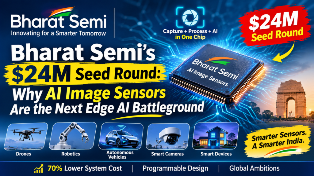
Bharat Semi, a New Delhi chip startup, has raised a $24 million all-equity seed round to build AI image sensors that capture, process and run AI on a single chip. Co-founder Vrinda Kapoor told TechCrunch that the integrated design could cut system costs by at least 70% compared with setups that use a separate image sensor, image signal processor and system-on-chip. If that claim survives production, it explains why this round matters well beyond India.
For a founder, engineer or student watching where AI hardware is heading, the story is a useful case study. Cameras and sensors are the eyes of every robot, drone, vehicle and smart device, yet most of them still stream raw data to some other chip to be understood. Bharat Semi wants the understanding to happen at the sensor itself. This guide explains what was announced, how AI image sensors work, what the numbers do and do not prove, and what the deal says about India’s fast-growing chip-design ecosystem.
Quick Answer: What Did Bharat Semi Announce?
Bharat Semi announced a $24 million seed round on November 15, 2026, to develop programmable image sensors for customers in the United States and other global markets. TechCrunch broke the news, and outlets including Entrepreneur India, Business Standard and YourStory followed with additional detail. The company is described as pre-revenue, with sensor prototypes still in development.
Key facts at a glance
- Amount: $24 million, all-equity seed round
- Lead investors: Info Edge Group, South Park Commons and Indus Bridge Ventures
- Other participants: Valour Capital, Micromax, Gaingels and individual investors
- Headquarters: New Delhi, with a US engineering presence in Santa Clara
- Team size: About 75 people across India and the United States
- Product: Programmable image sensors that combine capture, processing and AI on one chip
- Claimed benefit: System costs cut by at least 70% versus separate three-chip setups
- Early customers: Design wins with General Atomics and Kaynes Semicon
- Timeline: Second-generation sensors at prototype stage by mid-2027 and with customers by the end of 2027
- Business model: Fabless for the sensor business, meaning it designs chips and software while outsourcing manufacturing
What Are AI Image Sensors?
Definition
AI image sensors are image sensors that do more than capture light. They pair the pixel array with on-chip processing and machine-learning inference, so the device can interpret a scene, such as spotting an object, a movement or an anomaly, before raw data ever leaves the chip.
Expansion: the old pipeline versus the new one
In a conventional camera system, three separate components share the work. The image sensor converts light into raw digital data. An image signal processor, or ISP, cleans and formats that data. A system-on-chip, or SoC, then runs the AI models that decide what the picture means. Every handoff between those parts costs power, adds delay, takes up board space and increases the bill of materials.
AI image sensors collapse that chain. By putting capture, processing and inference on one piece of silicon, they aim to reduce cost, power draw and latency at the same time. Bharat Semi’s pitch adds a second twist: its sensors are programmable, so customers can change what the chip does through software instead of waiting for a new chip.
Why “programmable” matters
Fixed-function sensors are efficient but rigid. A programmable design lets one chip serve a drone today and a factory camera tomorrow. For a young company, that flexibility helps spread the very high cost of chip development across several markets rather than betting everything on one product.
How Do AI Image Sensors Cut System Costs by 70%?
Short answer: by replacing a three-part stack with a single chip and removing the engineering that connects the parts. Kapoor’s estimate, as reported by TechCrunch, is a reduction of at least 70%. Treat that number as a company claim until independent customers publish results from shipping products.
Based on how camera systems are built, the likely sources of savings are:
- Fewer chips: One device replaces a sensor, an ISP and an SoC, which shrinks the bill of materials.
- Less data movement: Moving high-resolution video between chips burns power. Processing at the source avoids much of it.
- Simpler boards: Fewer components mean fewer connections, smaller boards and shorter design cycles.
- Lower power budgets: Battery-powered devices such as drones and small robots benefit most when processing stays local.
These are analytical expectations, not company-published figures. They explain why the 70% claim is plausible in direction, even though the exact size of the saving will depend on the product and the customer.
Comparison: Conventional Camera Stack vs Integrated AI Image Sensors
| Factor | Conventional stack | Integrated AI image sensors |
|---|---|---|
| Components | Separate sensor, ISP and SoC | Capture, processing and AI on one chip |
| Data path | Raw data moves between chips | Data is interpreted at the source |
| System cost | Higher, with three parts to buy and integrate | At least 70% lower, per Bharat Semi’s claim |
| Power use | Higher because of data movement | Lower in principle, especially for battery devices |
| Flexibility | Depends on the SoC software | Programmable at the sensor itself |
| Maturity | Proven, widely deployed | Early, with prototypes still in development |
| Supply chain | Several vendors | One design, manufacturing outsourced to foundries |
The last row of the table is the honest counterweight. The conventional approach is slow and expensive, but it is proven. The integrated approach is attractive, but Bharat Semi still has to show it in volume.
Who Is Bharat Semi?
Founders and team
Bharat Semi was founded by Vrinda Kapoor, Vinayak Dalmia and Mukul Sarkar, according to a 2024 Business Standard profile. Kapoor and Dalmia are the two co-founders quoted in the funding coverage. The technical team also includes Boyd Fowler, a former chief technology officer of image-sensor maker OmniVision, which gives the startup credibility in a field where veteran sensor designers are scarce.
The company is described as nearly five years old and pre-revenue. It employs about 75 people, including 10 to 12 in Santa Clara, who handle engineering and business development.
A founder’s view on where sensors are going
Dalmia argued that growth in the sensor market will increasingly come from capturing data for machines rather than for people. Much of that data may never be seen by a human, yet it will drive AI at the edge. Kapoor framed the opportunity for India differently: as AI moves into the physical world and global supply chains are rebuilt, she sees room for an Indian company to build a globally relevant product business.
Who Backed the Round, and Why It Matters
The round was led by Info Edge Group, South Park Commons and Indus Bridge Ventures. Valour Capital, Micromax, Gaingels and individual investors also took part. South Park Commons general partner Prateek Mehta said the company is tackling how Physical AI actually gets built.
There is one more detail worth noting. Mint reported, as summarized by Lapaas Voice, that Bharat Semi first aimed to raise roughly $10 million to $15 million and lifted its target to around $25 million after investor interest grew. A round that expands mid-raise suggests demand from investors for AI hardware stories, though it says nothing yet about customer revenue.
Where Will the $24 Million Go?
Short answer: into people, product and customers. Bharat Semi plans to expand its engineering teams, particularly in the United States, complete product development and push its sensors toward the market. The funding will also accelerate a new family of products and support go-to-market work with global customers.
For a fabless chip company, the money matters in a specific way. Design tools, engineering talent and chip “tape-outs,” the stage when a design is sent to a foundry, consume most of the budget. Reporting on the round notes that seed funding of this size still may not be enough to fulfil mass orders, so a larger raise later is likely if early designs succeed.
Design Wins: General Atomics and Kaynes Semicon
Kapoor said Bharat Semi has secured design wins with two customers: General Atomics, a US defence and aerospace company, and Kaynes Semicon in India. A design win means a customer has chosen a chip for a future product. It is a meaningful signal, yet it is not revenue, because the product must still ship and sell.
Coverage of the round points to smart homes and aerospace as target areas for upcoming sensors. The pairing of a US defence customer and an Indian semiconductor firm also shows the company is trying to build credibility on both sides of its two-country footprint.
The Space Force Fab Project: Why It Is Separate
Many readers know Bharat Semi from a different story. In 2024, the company announced plans for a semiconductor fabrication project in India, built around a technology partnership that includes the US Space Force and the Indian firm 3rdiTech, with support from the India Semiconductor Mission.
Kapoor said that project is still in development, is separate from the sensor business and will not be funded by this seed round. For the sensor line, Bharat Semi plans to stay fabless, outsourcing manufacturing while it focuses on semiconductor design and software. Investors reading the round should treat these as two distinct bets.
Why Physical AI Is Pulling Demand Toward the Sensor
Definition: what is Physical AI?
Physical AI describes machines that use artificial intelligence to perceive and act in the real world. Robots, vehicles, drones and smart cameras are all examples. Each one needs to see before it can decide, which makes the image sensor the first link in the chain.
Question: Why process data at the sensor instead of the cloud?
Direct answer: because latency, bandwidth, power and privacy all improve when data is interpreted where it is captured. A robot avoiding an obstacle cannot wait for a round trip to a remote server. A battery-powered camera cannot afford to stream continuous video. A device that sends only conclusions, not raw footage, also exposes less private data. These are the pressures that make AI image sensors commercially interesting.
Where Bharat Semi is aiming
Bharat Semi says it wants to become the sensor layer for Physical AI across cameras, robots, vehicles, drones and other machines. That is an ambitious target for a company that has not yet shipped a product. It also puts the startup in a crowded field, because established chipmakers are adding on-sensor AI features of their own, such as STMicroelectronics’ vibration sensor with in-sensor AI.
India’s Chip-Design Startup Landscape
Bharat Semi’s round lands during a boom in Indian chip design. According to Tracxn data cited by YourStory, Indian semiconductor companies have attracted $1.4 billion in cumulative equity funding, with $701 million, nearly half, raised since 2025. The same report described a Semicon 2.0 blueprint worth Rs 1,27,500 crore, including venture-capital matching for chip startups. It also said 24 design startups have been approved for government support and 15 of them have raised venture funding.
Programmes aimed at talent are scaling too. Government figures cited in coverage say the Design Linked Incentive scheme has approved 23 chip-design projects and supported more than 70 firms with tools. Under the Chips to Startup programme, 71 academic institutions have completed 245 chip design tape-outs.
Comparison: Bharat Semi versus other Indian edge-AI chip startups
| Startup | Base | Latest reported round | Focus |
|---|---|---|---|
| Bharat Semi | New Delhi | $24M seed (Nov 2026) | Programmable AI image sensors |
| Sensesemi | Bengaluru | Rs 25 crore, about $2.75M seed (Jan 2026) | Edge-AI SoC with analog inference |
| Netrasemi | Kerala | About $12M Series A (July 2025), led by Zoho and Unicorn India Ventures | Edge-AI chips for video analytics and IoT sensors |
| HrdWyr | India | $13M | AI-native system-on-chip products |
At roughly nine times Sensesemi’s seed and double Netrasemi’s Series A, Bharat Semi’s round is large by Indian seed standards. Whether it translates into a lead depends on execution, since all four companies are still early.
Risks and Open Questions
A balanced reading of the news requires naming what is still unproven:
- Pre-revenue status: Prototypes are still in development, and commercial production is targeted for 2027.
- An unverified headline number: The 70% cost reduction is the company’s own estimate.
- Foundry dependence: A fabless model depends on outside manufacturers for capacity and pricing.
- Competition: Incumbent sensor and semiconductor firms have scale, customer relationships and their own AI roadmaps.
- Timeline risk: Chip schedules slip often, and a mid-2027 prototype target for the second generation leaves little margin.
None of these points cancel the opportunity. They are the questions to watch as the company reports its first customer results.
What This Means for Students and Freshers in India
For readers in Bhubaneswar and across Odisha, the practical lesson is about skills rather than headlines. Companies building AI image sensors need people who combine hardware and machine learning. The following areas look especially relevant:
- Digital design and verification: RTL design, SystemVerilog and verification methods
- Embedded and edge ML: Running compact models on constrained devices
- Computer vision fundamentals: Imaging pipelines, noise, exposure and calibration
- Firmware and hardware-software co-design: Making programmable chips usable
- Analog and mixed-signal basics: Because the sensor is where light becomes data
You do not need a fab to start. FPGA boards, open-source toolchains and small vision models let a student build a portfolio project that mirrors the sensor-plus-AI idea. The government figures above also show that academic tape-out programmes exist, so college-level chip design is a real path rather than a theory.
Frequently Asked Questions
How much did Bharat Semi raise?
Bharat Semi raised $24 million in an all-equity seed round, announced on November 15, 2026.
Who invested in the round?
Info Edge Group, South Park Commons and Indus Bridge Ventures led it. Valour Capital, Micromax, Gaingels and individual investors participated.
What are AI image sensors?
They are image sensors that combine image capture, signal processing and AI inference on one chip, so a device can interpret a scene without sending raw data to separate processors.
Is Bharat Semi building a chip fabrication plant with this money?
No. Kapoor said the seed round will not fund the separate fabrication project announced in 2024. The sensor business will remain fabless.
When will the products reach customers?
Second-generation sensors are expected at prototype stage by mid-2027 and with customers by the end of 2027. Commercial production is targeted for 2027.
Who are Bharat Semi’s early customers?
The company reports design wins with General Atomics and Kaynes Semicon. These are customer selections, not yet revenue.
Key Takeaways
- Bharat Semi’s $24 million seed round backs a single-chip approach to AI image sensors.
- The claimed 70% system-cost reduction is promising but unverified.
- Design wins with General Atomics and Kaynes Semicon are early validation, not revenue.
- The Space Force fab project is separate and not funded by this round.
- India’s chip-design startups are attracting record funding, and talent demand will follow.
ଭାରତ ସେମି (Bharat Semi) ର ୨୪ ନିୟୁତ ଡଲାରର ‘ସିଡ୍ ରାଉଣ୍ଡ’ (ପ୍ରାରମ୍ଭିକ ପାଣ୍ଠି ସଂଗ୍ରହ): AI ଇମେଜ୍ ସେନ୍ସରଗୁଡ଼ିକ କାହିଁକି ‘ଏଜ୍ AI’ (Edge AI) କ୍ଷେତ୍ରରେ ପରବର୍ତ୍ତୀ ପ୍ରମୁଖ ପ୍ରତିଯୋଗିତାର କେନ୍ଦ୍ରବିନ୍ଦୁ ପାଲଟିବ?
ନୂଆଦିଲ୍ଲୀସ୍ଥିତ ଚିପ୍ ଷ୍ଟାର୍ଟଅପ୍ ‘ଭାରତ ସେମି’ (Bharat Semi), AI ଇମେଜ୍ ସେନ୍ସର ବିକାଶ ପାଇଁ ୨୪ ନିୟୁତ ଡଲାରର ପାଣ୍ଠି ସଂଗ୍ରହ କରିଛି। ଏହି ସେନ୍ସରଗୁଡ଼ିକ ଗୋଟିଏ ଚିପ୍ ମଧ୍ୟରେ ଡାଟା ସଂଗ୍ରହ (capture), ପ୍ରକ୍ରିୟାକରଣ (process) ଏବଂ AI କାର୍ଯ୍ୟକାରୀ କରିବାର କ୍ଷମତା ରଖିବ। କମ୍ପାନୀର ସହ-ପ୍ରତିଷ୍ଠାତା ବୃନ୍ଦା କପୁର ‘ଟେକ୍କ୍ରଞ୍ଚ’ (TechCrunch) କୁ କହିଛନ୍ତି ଯେ, ଏହି ସମନ୍ୱିତ ଡିଜାଇନ୍ (integrated design) ବ୍ୟବହାର କଲେ ସିଷ୍ଟମ୍ ଖର୍ଚ୍ଚ ଅତିକମରେ ୭୦% ହ୍ରାସ ପାଇପାରିବ।
ଏହା ସେହି ସିଷ୍ଟମ୍ଗୁଡ଼ିକ ତୁଳନାରେ ଶସ୍ତା ହେବ, ଯେଉଁଥିରେ ଇମେଜ୍ ସେନ୍ସର, ଇମେଜ୍ ସିଗନାଲ୍ ପ୍ରୋସେସର୍ ଏବଂ ‘ସିଷ୍ଟମ୍-ଅନ୍-ଚିପ୍’ (SoC) ଅଲଗା ଅଲଗା ଭାବେ ବ୍ୟବହୃତ ହୁଏ। ଯଦି ଉତ୍ପାଦନ ପର୍ଯ୍ୟାୟରେ ଏହି ଦାବି ସତ୍ୟ ପ୍ରମାଣିତ ହୁଏ, ତେବେ ଏହା ସ୍ପଷ୍ଟ ହୋଇଯିବ ଯେ କାହିଁକି ଏହି ପାଣ୍ଠି ସଂଗ୍ରହ ଘଟଣାଟି କେବଳ ଭାରତ ପାଇଁ ନୁହେଁ, ବରଂ ବିଶ୍ୱସ୍ତରରେ ମଧ୍ୟ ଗୁରୁତ୍ୱପୂର୍ଣ୍ଣ ଅଟେ।
AI ହାର୍ଡୱେର୍ କ୍ଷେତ୍ର କେଉଁ ଦିଗରେ ଅଗ୍ରସର ହେଉଛି, ତାହା ଉପରେ ନଜର ରଖିଥିବା ଉଦ୍ୟୋକ୍ତା, ଇଞ୍ଜିନିୟର କିମ୍ବା ଛାତ୍ରଛାତ୍ରୀଙ୍କ ପାଇଁ ଏହି ଘଟଣାକ୍ରମ ଏକ ଉପଯୋଗୀ ଅଧ୍ୟୟନ ବିଷୟ ହୋଇପାରେ। କ୍ୟାମେରା ଏବଂ ସେନ୍ସରଗୁଡ଼ିକ ହେଉଛି ରୋବଟ୍, ଡ୍ରୋନ୍, ଯାନବାହାନ ଏବଂ ସ୍ମାର୍ଟ ଡିଭାଇସ୍ଗୁଡ଼ିକର ‘ଆଖି’ ସଦୃଶ; ତଥାପି, ଏଗୁଡ଼ିକ ମଧ୍ୟରୁ ଅଧିକାଂଶ କେବଳ କଞ୍ଚା ତଥ୍ୟ (raw data) ଅନ୍ୟ ଏକ ଚିପ୍କୁ ପଠାଇଥାନ୍ତି, ଯେଉଁଠାରେ ସେହି ତଥ୍ୟର ବିଶ୍ଳେଷଣ କରାଯାଏ। କିନ୍ତୁ ‘ଭାରତ ସେମି’ ଚାହେଁ ଯେ, ତଥ୍ୟର ବିଶ୍ଳେଷଣ ବା ବୁଝାମଣା ସେନ୍ସର ନିଜ ଭିତରେ ହିଁ ହେଉ। ଏହି ଲେଖାରେ କ’ଣ ଘୋଷଣା କରାଯାଇଛି, AI ଇମେଜ୍ ସେନ୍ସର କିପରି କାମ କରେ, ଏହି ସଂଖ୍ୟାଗୁଡ଼ିକ କ’ଣ ପ୍ରମା ମୁଖ୍ୟ ତଥ୍ୟ ଏକ ନଜରରେ
ପରିମାଣ: ୨୪ ନିୟୁତ ଡଲାର (୨.୪ କୋଟି ଡଲାର), ସମ୍ପୂର୍ଣ୍ଣ ଇକ୍ୱିଟି-ଆଧାରିତ ‘ସିଡ୍ ରାଉଣ୍ଡ’ (ପ୍ରାରମ୍ଭିକ ପୁଞ୍ଜି ନିବେଶ)
ମୁଖ୍ୟ ନିବେଶକ: ଇନଫୋ ଏଜ୍ ଗ୍ରୁପ୍ (Info Edge Group), ସାଉଥ୍ ପାର୍କ କମନ୍ସ (South Park Commons) ଏବଂ ଇଣ୍ଡସ୍ ବ୍ରିଜ୍ ଭେଞ୍ଚର୍ସ (Indus Bridge Ventures)
ଅନ୍ୟ ଅଂଶଗ୍ରହଣକାରୀ: ଭାଲୋର୍ କ୍ୟାପିଟାଲ୍ (Valour Capital), ମାଇକ୍ରୋମ୍ୟାକ୍ସ (Micromax), ଗେନଜେଲ୍ସ (Gaingels) ଏବଂ ବ୍ୟକ୍ତିଗତ ନିବେଶକମାନେ
ମୁଖ୍ୟ କାର୍ଯ୍ୟାଳୟ: ନୂଆଦିଲ୍ଲୀ; ଏହା ସହିତ ଆମେରିକାର ସାଣ୍ଟା କ୍ଲାରା (Santa Clara) ଠାରେ ଇଞ୍ଜିନିୟରିଂ କାର୍ଯ୍ୟାଳୟ ରହିଛି
ଦଳର ଆକାର: ଭାରତ ଏବଂ ଆମେରିକା ମିଶି ପ୍ରାୟ ୭୫ ଜଣ କର୍ମଚାରୀ
ଉତ୍ପାଦ: ପ୍ରୋଗ୍ରାମଯୋଗ୍ୟ (programmable) ଇମେଜ୍ ସେନ୍ସର, ଯାହା ଗୋଟିଏ ଚିପ୍ ମଧ୍ୟରେ ଛବି ଗ୍ରହଣ (capture), ପ୍ରକ୍ରିୟାକରଣ (processing) ଏବଂ AI (କୃତ୍ରିମ ବୁଦ୍ଧିମତ୍ତା) କ୍ଷମତାକୁ ଏକତ୍ରିତ କରିଥାଏ
ଦାବି କରାଯାଉଥିବା ଲାଭ: ପୃଥକ ତିନି-ଚିପ୍ ବିଶିଷ୍ଟ ବ୍ୟବସ୍ଥା ତୁଳନାରେ ସିଷ୍ଟମ୍ ଖର୍ଚ୍ଚରେ ଅତିକମରେ ୭୦% ହ୍ରାସ
ପ୍ରାରମ୍ଭିକ ଗ୍ରାହକ: ଜେନେରାଲ୍ ଆଟୋମିକ୍ସ (General Atomics) ଏବଂ କେନ୍ସ ସେମିକନ୍ (Kaynes Semicon) ସହିତ ଡିଜାଇନ୍ ଚୁକ୍ତି ସ୍ଥାପିତ ହୋଇଛି
ସମୟସୀମା: ୨୦୨୭ ମସିହା ମଧ୍ୟଭାଗ ସୁଦ୍ଧା ଦ୍ୱିତୀୟ ପିଢ଼ିର ସେନ୍ସରଗୁଡ଼ିକ ପ୍ରୋଟୋଟାଇପ୍ (ନମୁନା) ପର୍ଯ୍ୟାୟରେ ପହଞ୍ଚିବ ଏବଂ ୨୦୨୭ ଶେଷ ସୁଦ୍ଧା ଗ୍ରାହକଙ୍କ ନିକଟରେ ଉପଲବ୍ଧ ହେବ
ବ୍ୟବସାୟ ମଡେଲ୍: ସେନ୍ସର ବ୍ୟବସାୟ ପାଇଁ ‘ଫ୍ୟାବଲେସ୍’ (fabless) ମଡେଲ୍; ଅର୍ଥାତ୍ କମ୍ପାନୀ ନିଜେ ଚିପ୍ ଏବଂ ସଫ୍ଟୱେର୍ ଡିଜାଇନ୍ କରେ, କିନ୍ତୁ ଉତ୍ପାଦନ କାର୍ଯ୍ୟ ଅନ୍ୟ ସଂସ୍ଥା ଦ୍ୱାରା କରାଯାଏ
AI ଇମେଜ୍ ସେନ୍ସର କ’ଣ?
ସଂଜ୍ଞା
AI ଇମେଜ୍ ସେନ୍ସରଗୁଡ଼ିକ ହେଉଛି ଏପରି ଇମେଜ୍ ସେନ୍ସର, ଯାହା କେବଳ ଆଲୋକ ଗ୍ରହଣ କରିବା ବ୍ୟତୀତ ଆହୁରି ଅଧିକ କାର୍ଯ୍ୟ କରିଥାଏ। ଏଗୁଡ଼ିକ ପିକ୍ସେଲ୍ ଆରେ (pixel array) ସହିତ ଚିପ୍ ମଧ୍ୟରେ ଥିବା ପ୍ରକ୍ରିୟାକରଣ ଏବଂ ମେସିନ୍ ଲର୍ଣ୍ଣିଂ (machine learning) କ୍ଷମତାକୁ ଯୋଡ଼ିଥାଏ। ଫ ଏକ ପ୍ରୋଗ୍ରାମଯୋଗ୍ୟ (programmable) ଡିଜାଇନ୍ ଯୋଗୁଁ ଗୋଟିଏ ଚିପ୍ ଆଜି ଏକ ଡ୍ରୋନ୍ରେ ଏବଂ ଆସନ୍ତାକାଲି ଏକ କାରଖାନା କ୍ୟାମେରାରେ ବ୍ୟବହୃତ ହୋଇପାରିବ। ଏକ ନୂତନ କମ୍ପାନୀ ପାଇଁ, ଏହି ନମନୀୟତା ଚିପ୍ ବିକାଶର ଅତ୍ୟଧିକ ଖର୍ଚ୍ଚକୁ ବିଭିନ୍ନ ବଜାର ମଧ୍ୟରେ ବାଣ୍ଟିବାରେ ସାହାଯ୍ୟ କରେ; ଏହା ଫଳରେ କମ୍ପାନୀକୁ କେବଳ ଗୋଟିଏ ଉତ୍ପାଦ ଉପରେ ସବୁକିଛି ନିର୍ଭର କରିବାକୁ ପଡ଼େ ନାହିଁ।
AI ଇମେଜ୍ ସେନ୍ସରଗୁଡ଼ିକ କିପରି ସିଷ୍ଟମ୍ ଖର୍ଚ୍ଚକୁ ୭୦% ପର୍ଯ୍ୟନ୍ତ ହ୍ରାସ କରନ୍ତି?
ସଂକ୍ଷିପ୍ତ ଉତ୍ତର: ତିନୋଟି ଅଲଗା ଅଂଶ (stack) ବଦଳରେ ଗୋଟିଏ ମାତ୍ର ଚିପ୍ ବ୍ୟବହାର କରି ଏବଂ ସେହି ଅଂଶଗୁଡ଼ିକୁ ଯୋଡ଼ିବା ପାଇଁ ଆବଶ୍ୟକ ହେଉଥିବା ଜଟିଳ ଇଞ୍ଜିନିୟରିଂକୁ ହଟାଇ ଦେଇ ଏହା ସମ୍ଭବ ହୁଏ। ‘ଟେକ୍କ୍ରଞ୍ଚ’ (TechCrunch) ରିପୋର୍ଟ ଅନୁଯାୟୀ, କପୁରଙ୍କ ଆକଳନ ଅନୁସାରେ ଖର୍ଚ୍ଚରେ ଅତିକମରେ ୭୦% ହ୍ରାସ ଘଟିପାରେ। ତେବେ, ଯେପର୍ଯ୍ୟନ୍ତ ଗ୍ରାହକମାନେ ବଜାରରେ ଉପଲବ୍ଧ ଉତ୍ପାଦଗୁଡ଼ିକର ବ୍ୟବହାର ପରେ ନିଜର ଫଳାଫଳ ପ୍ରକାଶ ନ କରନ୍ତି, ସେପର୍ଯ୍ୟନ୍ତ ଏହି ସଂଖ୍ୟାକୁ କେବଳ କମ୍ପାନୀର ଏକ ଦାବି ଭାବରେ ବିବେଚନା କରିବା ଉଚିତ୍।
କ୍ୟାମେରା ସିଷ୍ଟମ୍ଗୁଡ଼ିକର ଗଠନ ଶୈଳୀକୁ ଦେଖିଲେ, ନିମ୍ନଲିଖିତ କ୍ଷେତ୍ରଗୁଡ଼ିକରେ ଖର୍ଚ୍ଚ ସଞ୍ଚୟ ହେବାର ସମ୍ଭାବନା ରହିଛି:
କମ୍ ଚିପ୍ର ଆବଶ୍ୟକତା: ଗୋଟିଏ ଡିଭାଇସ୍ ସେନ୍ସର, ISP (ଇମେଜ୍ ସିଗନାଲ୍ ପ୍ରୋସେସର୍) ଏବଂ SoC (ସିଷ୍ଟମ୍-ଅନ୍-ଚିପ୍) – ଏହି ତିନୋଟିର ସ୍ଥାନ ନିଏ, ଯାହା ଫଳରେ ଉତ୍ପାଦନ ପାଇଁ ଆବଶ୍ୟକ ଉପାଦାନଗୁଡ଼ିକର ମୋଟ ଖର୍ଚ୍ଚ (bill of materials) କମିଯାଏ।
ଡାଟା ସ୍ଥାନାନ୍ତରଣରେ ହ୍ରାସ: ଚିପ୍ଗୁଡ଼ିକ ମଧ୍ୟରେ ଉଚ୍ଚ-ରିଜୋଲ୍ୟୁସନ୍ (high-resolution) ଭିଡିଓ ସ୍ଥାନାନ୍ତର କରିବା ପାଇଁ ଅଧିକ ଶକ୍ତି (power) ବ୍ୟୟ ହୁଏ। ତଥ୍ୟ ଉତ୍ପତ୍ତି ସ୍ଥାନରେ ହିଁ ପ୍ରୋସେସିଂ କରିବା ଦ୍ୱାରା ଏହି ଶକ୍ତି ବ୍ୟୟକୁ ବହୁଳ ଭାବରେ ରୋକାଯାଇପାରେ।
ସରଳ ବୋର୍ଡ ଡିଜାଇନ୍: କମ୍ ଉପାଦାନର ଅର୍ଥ ହେଉଛି କମ୍ ସଂଯୋଗ, ଛୋଟ ବୋର୍ଡ ଏବଂ ଡିଜାଇନ୍ ପ୍ରକ୍ରିୟାରେ ଲାଗୁଥିବା ସମୟର ହ୍ରାସ।
କମ୍ ଶକ୍ତି ବ୍ୟବହାର (ଗୋଟିଏ ଚିପ୍ରେ ସେନ୍ସର ଏବଂ AI (କୃତ୍ରିମ ବୁଦ୍ଧିମତ୍ତା)
ଡାଟା ପଥ (Data path) ଚିପ୍ଗୁଡ଼ିକ ମଧ୍ୟରେ କଞ୍ଚା ତଥ୍ୟ (raw data) ଚଳାଚଳ କରେ ଉତ୍ସ ସ୍ଥାନରେ ହିଁ ତଥ୍ୟର ବିଶ୍ଳେଷଣ କରାଯାଏ
ସିଷ୍ଟମ୍ ମୂଲ୍ୟ ଅଧିକ, କାରଣ ତିନୋଟି ଅଲଗା ଅଂଶ କିଣି ସେଗୁଡ଼ିକୁ ଏକତ୍ରିତ କରିବାକୁ ପଡ଼େ ଭାରତ ସେମି (Bharat Semi) ର ଦାବି ଅନୁଯାୟୀ, ଅତିକମରେ ୭୦% କମ୍
ବିଦ୍ୟୁତ୍ ବ୍ୟବହାର ତଥ୍ୟ ଚଳାଚଳ ଯୋଗୁଁ ଅଧିକ ମୂଳତଃ କମ୍, ବିଶେଷକରି ବ୍ୟାଟେରୀ ଚାଳିତ ଉପକରଣ ପାଇଁ
ନମନୀୟତା SoC (System on Chip) ସଫ୍ଟୱେର୍ ଉପରେ ନିର୍ଭର କରେ ସେନ୍ସର ନିଜ ଭିତରେ ହିଁ ପ୍ରୋଗ୍ରାମ (ନିର୍ଦ୍ଦେଶ) ଦିଆଯାଇପାରିବ
ପରିପକ୍ୱତା ପରୀକ୍ଷିତ ଏବଂ ବ୍ୟାପକ ଭାବରେ ବ୍ୟବହୃତ ପ୍ରାରମ୍ଭିକ ପର୍ଯ୍ୟାୟ, ପ୍ରୋଟୋଟାଇପ୍ (ନମୁନା) ବିକାଶଧୀନ ଅବସ୍ଥାରେ ଅଛି
ଯୋଗାଣ ଶୃଙ୍ଖଳା (Supply chain) ଅନେକ ବିକ୍ରେତା (vendors) ଗୋଟିଏ ଡିଜାଇନ୍, କିନ୍ତୁ ଉତ୍ପାଦନ ଅନ୍ୟ କମ୍ପାନୀ (foundries) ଦ୍ୱାରା କରାଯାଏ
ସାରଣୀର ଶେଷ ଧାଡ଼ିଟି ଏକ ବାସ୍ତବବାଦୀ ତୁଳନା ପ୍ରଦାନ କରେ। ପାରମ୍ପାରିକ ପଦ୍ଧତି ଧୀର ଏବଂ ବ୍ୟୟବହୁଳ, କିନ୍ତୁ ଏହା ପରୀକ୍ଷିତ ଏବଂ ନିର୍ଭରଯୋଗ୍ୟ। ଏକୀକୃତ (integrated) ପଦ୍ଧତିଟି ଆକର୍ଷଣୀୟ, କିନ୍ତୁ ଭାରତ ସେମିକୁ ଏହା ବ୍ୟାପକ ସ୍ତରରେ ସଫଳତାର ସହ ପ୍ରଦର୍ଶନ କରିବାକୁ ବାକି ଅଛି।
ଭାରତ ସେମି (Bharat Semi) କିଏ?
ପ୍ରତିଷ୍ଠାତା ଏବଂ ଦଳ
‘ବିଜନେସ୍ ଷ୍ଟାଣ୍ଡାର୍ଡ’ର ୨୦୨୪ ମସିହାର ଏକ ରିପୋର୍ଟ ଅନୁଯାୟୀ, ଭାରତ ସେମିକୁ ବୃନ୍ଦା କପୁର, ବିନାୟକ ଦାଲମିଆ ଏବଂ ମୁକୁଳ ସରକାର ପ୍ରତିଷ୍ଠା କରିଥିଲେ। ପାଣ୍ଠି ସଂଗ୍ରହ ସମ୍ବନ୍ଧୀୟ ଖବରରେ କପୁର ଏବଂ ଦାଲମିଆଙ୍କୁ ସହ-ପ୍ରତିଷ୍ଠାତା ଭାବରେ ଉଲ୍ଲେଖ କରାଯାଇଛି। ଏହାର ବୈଷୟିକ ଦଳରେ ବଏଡ୍ ଫାଉଲର୍ ମଧ୍ୟ ଅଛନ୍ତି, ଯିଏ ଇମେଜ୍-ସେନ୍ସର ନିର୍ମାତା ‘ଓମ୍ନିଭିଜନ୍’ (OmniVision) ର ପୂର୍ବତନ ମୁଖ୍ୟ ବୈଷୟିକ ଅଧିକାରୀ (CTO) ଥିଲେ। ଏହା ଏହି ଷ୍ଟାର୍ଟଅପ୍କୁ ଏକ ବିଶେଷ ବିଶ୍ୱସନୀୟତା ପ୍ରଦାନ କରେ, କାରଣ ଏହି କ୍ଷେତ୍ରରେ ଅଭିଜ୍ଞ ସେନ୍ସର ଡିଜାଇନର୍ଙ୍କ ସଂଖ୍ୟା ବହୁତ କମ୍।
ଏହି କମ୍ପାନୀ ପ୍ରାୟ ପାଞ୍ଚ ବ ‘ସାଉଥ୍ ପାର୍କ କମନ୍ସ’ (South Park Commons) ର ଜେନେରାଲ୍ ପାର୍ଟନର ପ୍ରତୀକ ମେହେଟ୍ଟା କହିଛନ୍ତି ଯେ, କମ୍ପାନୀ ‘ଫିଜିକାଲ୍ ଏଆଇ’ (Physical AI) ବା ଭୌତିକ କୃତ୍ରିମ ବୁଦ୍ଧିମତ୍ତା ପ୍ରଣାଳୀକୁ ପ୍ରକୃତରେ କିପରି ନିର୍ମାଣ କରାଯାଇପାରିବ, ସେହି ଦିଗରେ କାମ କରୁଛି।
ଏଠାରେ ଆଉ ଏକ ଗୁରୁତ୍ୱପୂର୍ଣ୍ଣ ବିଷୟ ଅଛି। ‘ମିଣ୍ଟ’ (Mint) ର ରିପୋର୍ଟ ଅନୁଯାୟୀ (ଯାହାକୁ ‘ଲାପାସ୍ ଭଏସ୍’ (Lapaas Voice) ସାରାଂଶ ଆକାରରେ ପ୍ରକାଶ କରିଛି), ‘ଭାରତ ସେମି’ (Bharat Semi) ପ୍ରାରମ୍ଭରେ ପ୍ରାୟ ୧୦ ରୁ ୧୫ ନିୟୁତ ଡଲାର ସଂଗ୍ରହ କରିବାକୁ ଲକ୍ଷ୍ୟ ରଖିଥିଲା। କିନ୍ତୁ ନିବେଶକମାନଙ୍କ ଆଗ୍ରହ ବଢ଼ିବା ପରେ ଏହି ଲକ୍ଷ୍ୟକୁ ବଢ଼ାଇ ପ୍ରାୟ ୨୫ ନିୟୁତ ଡଲାର କରାଯାଇଥିଲା। ପାଣ୍ଠି ସଂଗ୍ରହ ପ୍ରକ୍ରିୟା ଚାଲିଥିବା ସମୟରେ ଲକ୍ଷ୍ୟ ପରିମାଣ ବୃଦ୍ଧି ପାଇବା, ଏଆଇ ହାର୍ଡୱେର୍ (AI hardware) କ୍ଷେତ୍ରରେ ନିବେଶକମାନଙ୍କର ଚାହିଦା ଥିବା ସୂଚିତ କରେ; ଯଦିଓ ଏଥିରୁ ଗ୍ରାହକଙ୍କ ଠାରୁ ମିଳୁଥିବା ରାଜସ୍ୱ (revenue) ବିଷୟରେ କୌଣସି ସୂଚନା ମିଳେ ନାହିଁ।
ଏହି ୨୪ ନିୟୁତ ଡଲାର କେଉଁଠାରେ ଖର୍ଚ୍ଚ ହେବ?
ସଂକ୍ଷିପ୍ତ ଉତ୍ତର ହେଲା: କର୍ମଚାରୀ, ଉତ୍ପାଦ ଏବଂ ଗ୍ରାହକଙ୍କ ପାଇଁ। ‘ଭାରତ ସେମି’ ନିଜର ଇଞ୍ଜିନିୟରିଂ ଦଳକୁ ବିସ୍ତାର କରିବାକୁ (ବିଶେଷକରି ଆମେରିକାରେ), ଉତ୍ପାଦ ବିକାଶ କାର୍ଯ୍ୟ ସମ୍ପୂର୍ଣ୍ଣ କରିବାକୁ ଏବଂ ନିଜର ସେନ୍ସରଗୁଡ଼ିକୁ ବଜାରକୁ ଆଣିବାକୁ ଯୋଜନା କରୁଛି। ଏହି ପାଣ୍ଠି ନୂତନ ଉତ୍ପାଦଗୁଡ଼ିକର ବିକାଶକୁ ତ୍ୱରାନ୍ୱିତ କରିବ ଏବଂ ବିଶ୍ୱସ୍ତରୀୟ ଗ୍ରାହକଙ୍କ ପାଖରେ ଉତ୍ପାଦ ପହଞ୍ଚାଇବା (go-to-market) କାର୍ଯ୍ୟରେ ସହାୟକ ହେବ।
ଏକ ‘ଫ୍ୟାବଲେସ୍’ (fabless) ଚିପ୍ କମ୍ପାନୀ ପାଇଁ (ଯେଉଁ କମ୍ପାନୀ ନିଜେ ଚିପ୍ ତିଆରି କରେ ନାହିଁ, ବରଂ ଡିଜାଇନ୍ କରେ), ଅର୍ଥର ବ୍ୟବହାର ଏକ ନିର୍ଦ୍ଦିଷ୍ଟ ଢଙ୍ଗରେ ହୋଇଥାଏ। ଡିଜାଇନ୍ ଟୁଲ୍, ଇଞ୍ଜିନିୟରିଂ ପ୍ରତିଭା ଏବଂ ଚିପ୍ “ଟେପ୍-ଆଉଟ୍” (tape-outs) — ଅର୍ଥାତ୍ ଡିଜାଇନ୍କୁ ଉତ୍ପାଦନ କେନ୍ଦ୍ର ବା ‘ଫାଉଣ୍ଡ୍ରି’ (foundry) କୁ ପଠାଇବା ପ୍ରକ୍ରିୟା — ଏସବୁରେ ବଜେଟର ଅଧିକାଂଶ ଅଂଶ ଖର୍ଚ୍ଚ ହୋଇଯାଏ। ଏହି ପାଣ୍ଠି ସଂଗ୍ରହ ସମ୍ବନ୍ଧୀୟ ରି 2024 ମସିହାରେ, କମ୍ପାନୀ ଭାରତରେ ଏକ ସେମିକଣ୍ଡକ୍ଟର ନିର୍ମାଣ ପ୍ରକଳ୍ପ ପାଇଁ ଯୋଜନା ଘୋଷଣା କରିଥିଲା, ଯାହା ଏକ ପ୍ରଯୁକ୍ତିବିଦ୍ୟା ସହଭାଗୀତା ଉପରେ ନିର୍ମିତ, ଯେଉଁଥିରେ US ସ୍ପେସ୍ ଫୋର୍ସ ଏବଂ ଭାରତୀୟ ଫାର୍ମ 3rdiTech ଅନ୍ତର୍ଭୁକ୍ତ, ଭାରତ ସେମିକଣ୍ଡକ୍ଟର ମିଶନର ସହାୟତାରେ।
କପୁର କହିଛନ୍ତି ଯେ ପ୍ରକଳ୍ପ ଏପର୍ଯ୍ୟନ୍ତ ବିକାଶାଧୀନ ଅଛି, ସେନ୍ସର ବ୍ୟବସାୟରୁ ପୃଥକ ଏବଂ ଏହି ସୀମ ରାଉଣ୍ଡ ଦ୍ୱାରା ପାଣ୍ଠି ଯୋଗାଇ ଦିଆଯିବ ନାହିଁ। ସେନ୍ସର ଲାଇନ ପାଇଁ, ଭାରତ ସେମି ଫ୍ୟାବଲେସ୍ ରହିବାକୁ ଯୋଜନା କରୁଛି, ଯେତେବେଳେ ଏହା ସେମିକଣ୍ଡକ୍ଟର ଡିଜାଇନ୍ ଏବଂ ସଫ୍ଟୱେର୍ ଉପରେ ଧ୍ୟାନ ଦିଏ, ଆଉଟସୋର୍ସିଂ ଉତ୍ପାଦନ କରିବାକୁ। ରାଉଣ୍ଡ ପଢ଼ୁଥିବା ନିବେଶକମାନେ ଏଗୁଡ଼ିକୁ ଦୁଇଟି ଭିନ୍ନ ବାଜି ଭାବରେ ବିଚାର କରିବା ଉଚିତ।
କାହିଁକି ଭୌତିକ AI ସେନ୍ସର ଆଡକୁ ଚାହିଦା ଟାଣି ନେଉଛି
ପରିଭାଷା: ଭୌତିକ AI କ’ଣ?
ଭୌତିକ AI ଏପରି ମେସିନଗୁଡ଼ିକୁ ବର୍ଣ୍ଣନା କରେ ଯାହା ବାସ୍ତବ ଦୁନିଆରେ ବୁଝିବା ଏବଂ କାର୍ଯ୍ୟ କରିବା ପାଇଁ କୃତ୍ରିମ ବୁଦ୍ଧିମତ୍ତା ବ୍ୟବହାର କରେ। ରୋବୋଟ୍, ଯାନବାହାନ, ଡ୍ରୋନ୍ ଏବଂ ସ୍ମାର୍ଟ କ୍ୟାମେରା ସମସ୍ତ ଉଦାହରଣ। ପ୍ରତ୍ୟେକଙ୍କୁ ନିଷ୍ପତ୍ତି ନେବା ପୂର୍ବରୁ ଦେଖିବା ଆବଶ୍ୟକ, ଯାହା ପ୍ରତିଛବି ସେନ୍ସରକୁ ଶୃଙ୍ଖଳରେ ପ୍ରଥମ ଲିଙ୍କ କରିଥାଏ।
ପ୍ରଶ୍ନ: କ୍ଲାଉଡ୍ ବଦଳରେ ସେନ୍ସରରେ ଡାଟା ପ୍ରକ୍ରିୟାକରଣ କାହିଁକି?
ସିଧାସଳଖ ଉତ୍ତର: କାରଣ ଲାଟେନ୍ସି, ବ୍ୟାଣ୍ଡୱିଡଥ୍, ପାୱାର ଏବଂ ପିଯେଉଁଠାରେ ତଥ୍ୟ ସଂଗ୍ରହ କରାଯାଏ, ସେହି ସ୍ଥାନରେ ହିଁ ଯଦି ତାର ବିଶ୍ଳେଷଣ କରାଯାଏ, ତେବେ ଏହା କାର୍ଯ୍ୟଦକ୍ଷତା ଏବଂ ଗୋପନୀୟତା ଉଭୟରେ ଉନ୍ନତି ଆଣିଥାଏ। ଉଦାହରଣ ସ୍ୱରୂପ, କୌଣସି ବାଧାକୁ ଏଡ଼ାଇ ଚାଲୁଥିବା ଏକ ରୋବଟ୍, ଦୂରରେ ଥିବା ସର୍ଭରକୁ ତଥ୍ୟ ପଠାଇ ପୁନର୍ବାର ଉତ୍ତର ପାଇବା ପାଇଁ ଅପେକ୍ଷା କରିପାରିବ ନାହିଁ। ସେହିପରି, ବ୍ୟାଟେରୀ ଚାଳିତ କ୍ୟାମେରାଗୁଡ଼ିକ ମଧ୍ୟ କ୍ରମାଗତ ଭାବେ ଭିଡିଓ ଷ୍ଟ୍ରିମ୍ କରିବାକୁ ସକ୍ଷମ ହୁଅନ୍ତି ନାହିଁ। ଯେଉଁ ଉପକରଣଗୁଡ଼ିକ କେବଳ ବିଶ୍ଳେଷଣର ଫଳାଫଳ (conclusions) ପଠାନ୍ତି ଏବଂ ମୂଳ ତଥ୍ୟ (raw data) ପଠାନ୍ତି ନାହିଁ, ସେଗୁଡ଼ିକ ବ୍ୟକ୍ତିଗତ ତଥ୍ୟର ଗୋପନୀୟତାକୁ ଅଧିକ ସୁରକ୍ଷିତ ରଖନ୍ତି। ଏହି ସବୁ ଆବଶ୍ୟକତା କାରଣରୁ AI (କୃତ୍ରିମ ବୁଦ୍ଧିମତା) ଯୁକ୍ତ ଇମେଜ୍ ସେନ୍ସରଗୁଡ଼ିକ ବ୍ୟବସାୟିକ ଦୃଷ୍ଟିରୁ ଅତ୍ୟନ୍ତ ଆକର୍ଷଣୀୟ ହୋଇପାରିଛି।
‘ଭାରତ ସେମି’ (Bharat Semi) ର ଲକ୍ଷ୍ୟ
‘ଭାରତ ସେମି’ କହିଛି ଯେ ଏହା କ୍ୟାମେରା, ରୋବଟ୍, ଯାନବାହାନ, ଡ୍ରୋନ୍ ଏବଂ ଅନ୍ୟାନ୍ୟ ଯନ୍ତ୍ରପାତି କ୍ଷେତ୍ରରେ ‘ଫିଜିକାଲ୍ AI’ (Physical AI) ପାଇଁ ଏକ ‘ସେନ୍ସର ସ୍ତର’ (sensor layer) ଭାବରେ କାର୍ଯ୍ୟ କରିବାକୁ ଲକ୍ଷ୍ୟ ରଖିଛି। ଯେହେତୁ ଏହି କମ୍ପାନୀ ବର୍ତ୍ତମାନ ସୁଦ୍ଧା କୌଣସି ଉତ୍ପାଦ ବଜାରକୁ ଆଣିନାହିଁ, ତେଣୁ ଏହି ଲକ୍ଷ୍ୟ ବେଶ୍ ଉଚ୍ଚାଭିଳାଷୀ ଅଟେ। ଏହା ବ୍ୟତୀତ, ଏହି ଷ୍ଟାର୍ଟଅପ୍କୁ ଏକ ପ୍ରତିଯୋଗିତାମୂଳକ କ୍ଷେତ୍ରରେ କାମ କରିବାକୁ ପଡ଼ିବ, କାରଣ ବର୍ତ୍ତମାନର ପ୍ରତିଷ୍ଠିତ ଚିପ୍ ନିର୍ମାତାମାନେ ମଧ୍ୟ ନିଜ ଉତ୍ପାଦରେ AI ବୈଶିଷ୍ଟ୍ୟ ଯୋଡ଼ୁଛନ୍ତି। ଉଦାହରଣ ସ୍ୱରୂପ, STMicroelectronics (ଏସ୍.ଟି. ମାଇକ୍ରୋଇଲେକ୍ଟ୍ରୋନିକ୍ସ) ର ଭାଇବ୍ରେସନ୍ ସେନ୍ସରରେ ଏଭଳି AI ବୈଶିଷ୍ଟ୍ୟ ରହିଛି।
ଭାରତରେ ଚିପ୍-ଡିଜାଇନ୍ ଷ୍ଟାର୍ଟଅପ୍ କ୍ଷେତ୍ରର ସ୍ଥିତି
ଭାରତରେ ଚିପ୍ ଡିଜାଇନ୍ କ୍ଷେତ୍ରରେ ଏକ ବଡ଼ ଧରଣର ଅଭିବୃଦ୍ଧି ଦେଖାଯାଉଥିବା ବେଳେ ‘ଭାରତ ସେମି’ ପାଇଁ ଏହି ପାଣ୍ଠି ସଂଗ୍ରହ (funding) ପ୍ରକ୍ରିୟା ଆସିଛି। ‘ୟୋର୍ ଷ୍ଟୋରୀ’ (YourStory) ଦ୍ୱାରା ଉଦ୍ଧୃତ ‘ଟ୍ରାକ୍ସନ୍’ (Tracxn) ତଥ୍ୟ ଅନୁଯାୟୀ, ଭାର ତୁଳନା: ଭାରତ ସେମି (Bharat Semi) ଏବଂ ଅନ୍ୟାନ୍ୟ ଭାରତୀୟ ‘ଏଜ୍-ଏଆଇ’ (Edge-AI) ଚିପ୍ ଷ୍ଟାର୍ଟଅପ୍
ଷ୍ଟାର୍ଟଅପ୍ | ମୁଖ୍ୟ କାର୍ଯ୍ୟାଳୟ | ସର୍ବଶେଷ ପାଣ୍ଠି ସଂଗ୍ରହ (ରାଉଣ୍ଡ) | ମୁଖ୍ୟ ଲକ୍ଷ୍ୟ
ଭାରତ ସେମି (Bharat Semi) | ନୂଆଦିଲ୍ଲୀ | $୨୪ ନିୟୁତ ‘ସିଡ୍’ (Seed) ପାଣ୍ଠି (ନଭେମ୍ବର ୨୦୨୬) | ପ୍ରୋଗ୍ରାମେବଲ୍ AI ଇମେଜ୍ ସେନ୍ସର
ସେନ୍ସସେମି (Sensesemi) | ବେଙ୍ଗାଲୁରୁ | ୨୫ କୋଟି ଟଙ୍କା (ପ୍ରାୟ $୨.୭୫ ନିୟୁତ) ‘ସିଡ୍’ ପାଣ୍ଠି (ଜାନୁଆରୀ ୨୦୨୬) | ଆନାଲଗ୍ ଇନଫରେନ୍ସ (analog inference) ସହିତ ‘ଏଜ୍-ଏଆଇ’ SoC
ନେତ୍ରାସେମି (Netrasemi) | କେରଳ | ପ୍ରାୟ $୧୨ ନିୟୁତ ‘ସିରିଜ୍ A’ (Series A) ପାଣ୍ଠି (ଜୁଲାଇ ୨୦୨୫) – ଜୋହୋ (Zoho) ଏବଂ ୟୁନିକର୍ଣ୍ଣ ଇଣ୍ଡିଆ ଭେଞ୍ଚର୍ସଙ୍କ ନେତୃତ୍ୱରେ | ଭିଡିଓ ଆନାଲିଟିକ୍ସ ଏବଂ IoT ସେନ୍ସର ପାଇଁ ‘ଏଜ୍-ଏଆଇ’ ଚିପ୍
ହାର୍ଡୱାୟାର (HrdWyr) | ଭାରତ | $୧୩ ନିୟୁତ | AI-ଆଧାରିତ ‘ସିଷ୍ଟମ୍-ଅନ୍-ଚିପ୍’ (SoC) ଉତ୍ପାଦ
ସେନ୍ସସେମିର ‘ସିଡ୍’ ପାଣ୍ଠି ତୁଳନାରେ ପ୍ରାୟ ନଅ ଗୁଣ ଏବଂ ନେତ୍ରାସେମିର ‘ସିରିଜ୍ A’ ପାଣ୍ଠି ତୁଳନାରେ ଦ୍ୱିଗୁଣ ପାଣ୍ଠି ସଂଗ୍ରହ କରିଥିବାରୁ, ଭାରତ ସେମିର ଏହି ପାଣ୍ଠି ସଂଗ୍ରହ ଭାରତୀୟ ‘ସିଡ୍’ ମାନଦଣ୍ଡ ଅନୁଯାୟୀ ବେଶ୍ ବଡ଼ ଅଟେ। ଏହା କମ୍ପାନୀକୁ ବଜାରରେ ଅଗ୍ରଣୀ ସ୍ଥାନ ଦେବ କି ନାହିଁ, ତାହା କାର୍ଯ୍ୟକାରିତା ଉପରେ ନିର୍ଭର କରେ; କାରଣ ଏହି ଚାରୋଟିଯାକ କମ୍ପାନୀ ବର୍ତ୍ତମାନ ପ୍ରାରମ୍ଭିକ ପର୍ଯ୍ୟାୟରେ ଅଛନ୍ତି।
ଝୁଙ୍କି ଏବଂ ଅନିଶ୍ଚିତ ପ୍ରଶ୍ନଗୁଡ଼ିକ
ଏହି ଖବରକୁ ନିରପେକ୍ଷ ଭାବରେ ବିଚାର କରିବାକୁ ଗଲେ, କିଛି ବିଷୟ ଏପର୍ଯ୍ୟନ୍ତ ପ୍ରମାଣିତ ହୋଇନାହିଁ ବୋଲି ଉଲ୍ଲେଖ କରିବା ଆବଶ୍ୟକ:
ଆୟ ଆରମ୍ଭ ହୋଇନାହିଁ: ଉତ୍ପାଦର ନମୁନା (Prototypes) ବର୍ତ୍ତମାନ ବିକାଶ ପର୍ଯ୍ୟାୟରେ ଅଛି ଏବଂ ବ୍ୟବସାୟିକ ଉତ୍ପାଦନ ୨୦୨୭ ମସିହାରୁ ଆରମ୍ଭ ହେବାର ଲକ୍ଷ୍ୟ ରଖାଯାଇଛି।
ଦାବି କରାଯାଇଥିବା ସଂଖ୍ୟା ଯାଞ୍ଚ ହୋଇନାହିଁ: ଖର୍ଚ୍ଚ ୭୦% କମିଯିବ ବୋଲି ଯେଉଁ ଦାବି କରାଯାଇଛି, ତାହା କମ୍ପାନୀର ନିଜସ୍ୱ ଆକଳନ ମାତ୍ର।
ଉତ୍ପାଦନ ପାଇ ନିମ୍ନଲିଖିତ କ୍ଷେତ୍ରଗୁଡ଼ିକ ବିଶେଷ ଭାବରେ ପ୍ରାସଙ୍ଗିକ ମନେହୁଏ:
ଡିଜିଟାଲ୍ ଡିଜାଇନ୍ ଏବଂ ଯାଞ୍ଚ (Verification): RTL ଡିଜାଇନ୍, SystemVerilog ଏବଂ ଯାଞ୍ଚ ପଦ୍ଧତି।
ଏମ୍ବେଡେଡ୍ (Embedded) ଏବଂ ଏଜ୍ (Edge) ML: ସୀମିତ ସମ୍ବଳ ବିଶିଷ୍ଟ ଉପକରଣଗୁଡ଼ିକରେ ଛୋଟ କିମ୍ବା ସଂକ୍ଷିପ୍ତ ମଡେଲ୍ ଚଳାଇବା।
କମ୍ପ୍ୟୁଟର ଭିଜନ୍ର ମୌଳିକ ବିଷୟ: ଇମେଜିଙ୍ଗ୍ ପାଇପଲାଇନ୍, ନଏଜ୍ (noise), ଏକ୍ସପୋଜର୍ ଏବଂ କାଲିବ୍ରେସନ୍।
ଫାର୍ମୱେୟାର୍ ଏବଂ ହାର୍ଡୱେୟାର୍-ସଫ୍ଟୱେୟାର୍ ସହ-ଡିଜାଇନ୍ (Co-design): ପ୍ରୋଗ୍ରାମେବଲ୍ ଚିପ୍ଗୁଡ଼ିକୁ ବ୍ୟବହାରଯୋଗ୍ୟ କରିବା।
ଆନାଲଗ୍ ଏବଂ ମିକ୍ସଡ୍-ସିଗନାଲ୍ର ମୌଳିକ ଧାରଣା: କାରଣ ସେନ୍ସର (sensor) ସ୍ଥାନରେ ହିଁ ଆଲୋକ ତଥ୍ୟ (data) ରେ ପରିଣତ ହୋଇଥାଏ।
ଆରମ୍ଭ କରିବା ପାଇଁ ଆପଣଙ୍କୁ ଏକ ‘ଫ୍ୟାବ୍’ (ଚିପ୍ ନିର୍ମାଣ କାରଖାନା) ର ଆବଶ୍ୟକତା ନାହିଁ। FPGA ବୋର୍ଡ, ଓପନ୍-ସୋର୍ସ ଟୁଲ୍ଚେନ୍ ଏବଂ ଛୋଟ ଭିଜନ୍ ମଡେଲ୍ଗୁଡ଼ିକ ସାହାଯ୍ୟରେ ଜଣେ ଛାତ୍ର ଏପରି ଏକ ପ୍ରୋଜେକ୍ଟ (ପୋର୍ଟଫୋଲିଓ) ପ୍ରସ୍ତୁତ କରିପାରିବେ, ଯାହା ‘ସେନ୍ସର ଏବଂ AI’ ର ଧାରଣାକୁ ପ୍ରତିଫଳିତ କରେ। ଉପରୋକ୍ତ ସରକାରୀ ତଥ୍ୟରୁ ଜଣାପଡ଼େ ଯେ ଶିକ୍ଷାନୁଷ୍ଠାନଗୁଡ଼ିକ ପାଇଁ ‘ଟେପ୍-ଆଉଟ୍’ (tape-out) କାର୍ଯ୍ୟକ୍ରମ ରହିଛି; ତେଣୁ କଲେଜ ସ୍ତରରେ ଚିପ୍ ଡିଜାଇନ୍ କରିବା କେବଳ ଏକ ତତ୍ତ୍ୱ ନୁହେଁ, ବରଂ ଏକ ବାସ୍ତବ ପଥ ଅଟେ।
ସାଧାରଣତଃ ପଚରାଯାଉଥିବା ପ୍ରଶ୍ନ (FAQs)
ଭାରତ ସେମି (Bharat Semi) କେତେ ପୁଞ୍ଜି ସଂଗ୍ରହ କରିଛି?
ଭାରତ ସେମି, ୧୫ ନଭେମ୍ବର ୨୦୨୬ ରେ ଘୋଷଣା କରିଛି ଯେ ଏହା ଏକ ‘ସିଡ୍ ରାଉଣ୍ଡ’ (seed round) ମାଧ୍ୟମରେ ୨୪ ନିୟୁତ ଡଲାର୍ ପୁଞ୍ଜି ସଂଗ୍ରହ କରିଛି।
ଏହି ପୁଞ୍ଜି ନିବେଶରେ କିଏ ଅଂଶଗ୍ରହଣ କରିଥିଲେ?
Info Edge Group, South Park Commons ଏବଂ Indus Bridge Ventures ଏହାର ନେତୃତ୍ୱ ନେଇଥିଲେ। ଏହା ବ୍ୟତୀତ Valour Capital, Micromax, Gaingels ଏବଂ ଅନ୍ୟାନ୍ୟ ବ୍ୟକ୍ତିଗତ ନିବେଶକମାନେ ମଧ୍ୟ ଏଥିରେ ସାମିଲ ହୋଇଥିଲେ।
AI ଇମେଜ୍ ସେନ୍ସର କ’ଣ?
ଏଗୁଡ଼ିକ ହେଉଛି ଏପରି ଇମେଜ୍ ସେନ୍ସର ଯାହା ଗୋଟିଏ ଚିପ୍ ମଧ୍ୟରେ ଛବି ଗ୍ରହଣ କରିବା (image capture), ସି୨୦୨୭ ପାଇଁ ଲକ୍ଷ୍ୟ ରଖାଯାଇଛି।
ଭାରତ ସେମିର ପ୍ରାରମ୍ଭିକ ଗ୍ରାହକ କିଏ?
କମ୍ପାନୀ ଜେନେରାଲ ଆଟୋମିକ୍ସ ଏବଂ କେନ୍ସ ସେମିକନ ସହିତ ଡିଜାଇନ୍ ବିଜୟ ରିପୋର୍ଟ କରିଛି। ଏଗୁଡ଼ିକ ଗ୍ରାହକଙ୍କ ଚୟନ, ଏପର୍ଯ୍ୟନ୍ତ ରାଜସ୍ୱ ନୁହେଁ।
ପ୍ରମୁଖ ପ୍ରସଙ୍ଗ
ଭାରତ ସେମିର $୨୪ ନିୟୁତ ସିଡ୍ ରାଉଣ୍ଡ AI ପ୍ରତିଛବି ସେନ୍ସର ପାଇଁ ଏକକ-ଚିପ୍ ପଦ୍ଧତିକୁ ସମର୍ଥନ କରେ।
ଦାବି କରାଯାଇଥିବା ୭୦% ସିଷ୍ଟମ୍-ଖର୍ଚ୍ଚ ହ୍ରାସ ପ୍ରତିଶ୍ରୁତିପୂର୍ଣ୍ଣ କିନ୍ତୁ ଯାଞ୍ଚ କରାଯାଇନାହିଁ।
ଜେନେରାଲ ଆଟୋମିକ୍ସ ଏବଂ କେନ୍ସ ସେମିକନ ସହିତ ଡିଜାଇନ୍ ବିଜୟ ପ୍ରାରମ୍ଭିକ ବୈଧତା, ରାଜସ୍ୱ ନୁହେଁ।
ସ୍ପେସ୍ ଫୋର୍ସ ଫ୍ୟାବ୍ ପ୍ରୋଜେକ୍ଟ ପୃଥକ ଏବଂ ଏହି ରାଉଣ୍ଡ ଦ୍ୱାରା ପାଣ୍ଠି ଯୋଗାଇ ଦିଆଯାଇ ନାହିଁ।
ଭାରତର ଚିପ୍-ଡିଜାଇନ୍ ଷ୍ଟାର୍ଟଅପ୍ ରେକର୍ଡ ପାଣ୍ଠି ଆକର୍ଷିତ କରୁଛନ୍ତି, ଏବଂ ପ୍ରତିଭା ଚାହିଦା ଅନୁସରଣ କରିବ।