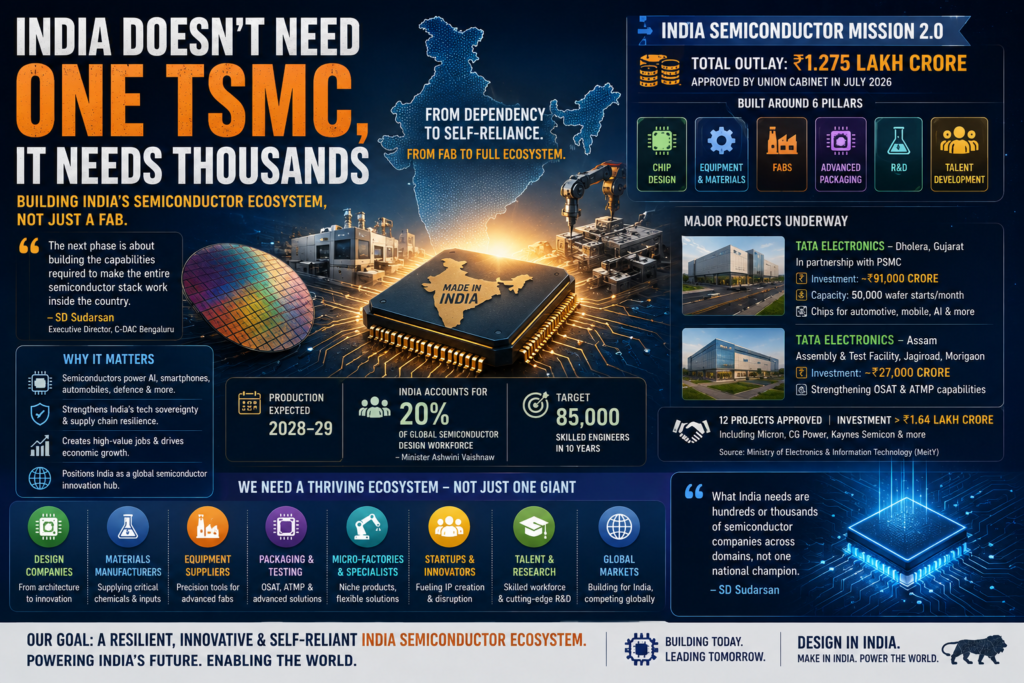
India’s semiconductor ambitions are entering a new phase: building a fab is no longer enough. The country now needs the materials, equipment, packaging, design capabilities, specialised suppliers, skilled workforce and homegrown intellectual property that can make an entire India semiconductor ecosystem work.
That is the central idea behind India’s transition from the first phase of its semiconductor mission to India Semiconductor Mission 2.0 (ISM 2.0). Rather than trying to create a single company that replicates Taiwan Semiconductor Manufacturing Company (TSMC), policymakers and industry experts increasingly see value in building a broad network of companies operating across the semiconductor value chain.
SD Sudarsan, Executive Director at C-DAC Bengaluru, argues that the next stage of India’s semiconductor journey must move beyond fabs and chip design. It needs to include semiconductor equipment, materials, advanced packaging, research, talent and smaller specialised manufacturers.
The shift matters because semiconductors are no longer just another manufacturing sector. They sit underneath AI systems, smartphones, automobiles, defence systems, electronics and increasingly strategic computing infrastructure.
So, can India build a globally competitive India semiconductor ecosystem without creating its own single TSMC?
The answer may depend less on finding one giant winner and more on creating hundreds or even thousands of specialised companies that collectively make the country more capable of designing, manufacturing, packaging and deploying chips.
India’s Semiconductor Mission Is Entering Its Second Phase
India’s first semiconductor push focused heavily on establishing the foundations: fabs, packaging facilities and chip-design capabilities. The next phase is broader, with the emphasis moving toward the ecosystem surrounding semiconductor manufacturing.
What is ISM 2.0?
ISM 2.0 is the expanded phase of India’s semiconductor programme, designed to scale existing initiatives while supporting more parts of the semiconductor value chain.
The Union Cabinet approved the expanded Semicon 2.0 programme in July 2026 with a total outlay of ₹1.275 lakh crore. According to the source material, the programme is structured around six pillars: chip design, equipment and materials, fabs, advanced packaging, research and development, and talent development.
That structure reveals something important. India is no longer approaching semiconductors simply as a race to build a fabrication plant.
Instead, the objective is becoming much closer to building an industrial network.
A semiconductor fab needs specialised chemicals. It needs equipment capable of extremely precise manufacturing. It needs engineers and technicians. It needs packaging and testing capabilities. It needs suppliers that can reliably deliver inputs and components.
If even one of these layers is weak, the manufacturing chain becomes dependent on external suppliers.
Why a fab alone is not enough
Question: Does building a semiconductor fab make a country self-sufficient in chips?
No. A fab is only one part of the semiconductor manufacturing process.
Sudarsan points out that semiconductor manufacturing requires a large number of supporting capabilities, particularly materials and equipment. A typical fab can require hundreds of unique chemicals, many of which are subject to different regulatory categories, import restrictions and export controls.
That creates a challenge for India.
If a domestic fab still depends heavily on imported materials, equipment or specialised technologies, the country may have manufacturing capacity without having complete control over the underlying supply chain.
That is why the India semiconductor ecosystem increasingly matters as much as individual fabs.
India Already Has Major Semiconductor Projects
India is not starting from zero.
The first phase of the semiconductor mission has already produced multiple large projects, including major investments in fabrication, assembly and testing. These projects are intended to create the initial industrial base on which the wider India semiconductor ecosystem can develop.
One of the biggest examples is in Dholera, Gujarat, where Tata Electronics is developing a semiconductor fab in partnership with Taiwan’s Powerchip Semiconductor Manufacturing Corporation (PSMC). The project represents an investment of around ₹91,000 crore and is planned for a capacity of 50,000 wafer starts per month. The chips are intended for applications including automobiles, mobile devices and AI.
Another major project is being developed in Assam.
Tata Electronics is building a ₹27,000-crore semiconductor assembly and test facility in Jagiroad, Morigaon. Together, such projects demonstrate that India’s strategy is beginning to span multiple stages of the semiconductor value chain.
The government says the first phase has already approved 12 semiconductor projects with investments exceeding ₹1.64 lakh crore. These include Micron’s packaging facility, Tata Electronics’ silicon fab with PSMC, and OSAT projects from CG Power and Kaynes Semicon.
However, these facilities are not expected to become fully operational immediately.
According to Sudarsan, actual production is expected around 2028–29. That means the next few years will be critical not just for construction, but also for building the workforce, suppliers and operational expertise required to make the projects successful.
The Missing Piece Is the Ecosystem Around the Fab
Imagine a semiconductor fab as the centre of a city.
The fab may be the most visible building, but it cannot function without roads, electricity, water, suppliers, workers, logistics, maintenance companies, laboratories and specialised services.
The same logic applies to semiconductor manufacturing.
Definition , Semiconductor ecosystem: A semiconductor ecosystem is the connected network of companies, infrastructure, talent, technologies and institutions involved in designing, manufacturing, packaging, testing and supplying semiconductor products.
For India, building this network could be more strategically important than simply attracting one enormous manufacturing project.
The country needs companies that can manufacture semiconductor-grade materials. It needs equipment suppliers. It needs advanced packaging specialists. It needs design firms that can turn architectures into manufacturable chips. It needs testing capabilities and engineers who understand production at scale.
That is the difference between having a semiconductor project and having a functioning India semiconductor ecosystem.
The materials problem
Question: Why are semiconductor materials so important?
Because fabs cannot manufacture chips without highly specialised inputs.
Sudarsan highlights the complexity of semiconductor materials, noting that fabs may require hundreds of different chemicals. These materials can involve hazardous-substance regulations as well as import and export controls.
That means India needs more than manufacturing buildings.
It needs companies capable of supplying critical inputs consistently and safely. Developing those businesses could create an entirely new industrial layer around semiconductor manufacturing.
This is where smaller Indian companies could become strategically important.
India Has a Strong Starting Point: Chip Design Talent
One of India’s biggest advantages is not necessarily manufacturing experience. It is engineering and chip-design talent.
Union Electronics and IT Minister Ashwini Vaishnaw has said that India accounts for 20% of the global semiconductor design workforce. He has also set a target of developing a pool of 85,000 skilled engineers over 10 years.
Sudarsan estimates that around 25–30% of global chip-design activity is carried out in India, although much of this work is conducted through global companies’ engineering centres and Global Capability Centres.
That distinction is important.
India has significant design expertise, but design activity does not automatically translate into Indian-owned semiconductor products.
The next challenge is converting technical capability into intellectual property and commercially successful products.
From architecture to manufactured chip
Question: What is India’s biggest chip-design challenge?
The challenge is moving from designing a chip architecture to actually implementing that architecture for a specific manufacturing process.
Sudarsan describes India as being strong in front-end design, but says the country must strengthen implementation and back-end design capabilities. Back-end design involves translating a chip architecture into something that can actually be manufactured using a particular fabrication process.
That requires specialised knowledge.
And that knowledge is becoming deeper among Indian students and engineers.
Sudarsan says that discussions around VLSI design in academic institutions have become more specialised, with engineers increasingly distinguishing between front-end and back-end design and focusing on areas such as analogue, digital, RF and mixed-signal design.
The implication is encouraging: India is developing technical depth alongside its growing manufacturing ambitions.
But technical skill alone will not be enough.
Manufacturing requires consistency, discipline and ownership. Producing one successful prototype is very different from manufacturing millions of identical chips with reliable quality.
Why India Does Not Need to Copy TSMC
TSMC is an obvious reference point whenever semiconductor manufacturing is discussed.
The Taiwanese company has become the dominant example of a successful contract chip manufacturer. But attempting to reproduce TSMC exactly may not be the best strategy for India.
Question: Does India need one semiconductor giant like TSMC?
Not necessarily. The source argues for a much broader network of companies, including smaller specialised manufacturers and potentially micro-factories.
Sudarsan believes India should eventually have hundreds or thousands of semiconductor companies across different domains, rather than depending on one national champion.
That could produce a very different model of semiconductor growth.
Instead of one organisation trying to control an enormous portion of the industry, specialised companies could focus on particular products, materials, manufacturing processes or applications.
| Model | Core idea | Potential advantage |
| Single national champion | Build one dominant semiconductor company | Concentrated scale and resources |
| Large fab-led ecosystem | Build major fabs and attract suppliers | Strong manufacturing base |
| Distributed ecosystem | Develop hundreds or thousands of specialised companies | Diversification and resilience |
| Micro-factory model | Smaller facilities focused on specific products | Flexible specialised manufacturing |
The distributed model could also make the India semiconductor ecosystem more resilient.
If the country has multiple suppliers and manufacturers across different regions and technologies, a problem at one company does not necessarily disrupt the entire system.
That does not mean large fabs are unimportant.
They remain essential for high-volume manufacturing.
The point is that fabs should become anchors around which a larger industrial network develops.
Advanced Packaging Could Become a Major Opportunity
Chip manufacturing does not end when a semiconductor wafer is produced.
The chips also need to be packaged and tested before they can be integrated into electronic products.
India’s current semiconductor projects therefore include significant activity around OSAT and ATMP, which cover semiconductor assembly, packaging and testing.
These capabilities are important because advanced packaging increasingly influences how chips perform and how different components can be integrated.
For India, packaging could offer a route to develop semiconductor manufacturing expertise while the country continues building more advanced fabrication capabilities.
But packaging should not be treated as the final destination.
The broader objective is to build capabilities across materials, equipment, process control, manufacturing, design and talent.
That is what turns individual semiconductor projects into a functioning India semiconductor ecosystem.
ISM 2.0 Could Change Semiconductor Startup Funding
Another potentially important development is the role of government capital.
ISM 2.0 is exploring an equity co-investment approach for semiconductor startups. According to ISM CEO Amitesh Kumar Sinha, the government plans to co-invest alongside eligible private or venture-capital investors and eventually exit those investments as companies mature.
The idea is not simply to give startups money.
It is to bring commercial investors into the process.
Sudarsan describes a possible matching-grant mechanism in which private investors conduct due diligence and invest in a semiconductor company, with the government potentially matching that investment.
For example, if private investors provide an amount represented as X, government matching could potentially make the total investment 2X.
That could be particularly useful for semiconductor startups because hardware businesses typically require much more capital and longer development timelines than conventional software startups.
A semiconductor company may need years of engineering, verification, prototyping and manufacturing work before it can generate meaningful revenue.
A funding model that recognises this reality could help more Indian chip companies survive the journey from idea to commercial product.
India’s Semiconductor Challenge Is Now About Manufacturing Excellence
Designing a chip is difficult.
Manufacturing millions of them consistently is a different problem.
This distinction may become one of the biggest tests for India.
India already has significant strengths in software, engineering and research. But semiconductor manufacturing demands an extraordinary level of precision and repeatability.
Question: What separates semiconductor research from semiconductor manufacturing?
Manufacturing requires the ability to repeatedly produce chips with consistent quality and high yields. A technically impressive design is not enough if the manufacturing process cannot reliably reproduce it at commercial scale.
That is why equipment and process control are so important.
Sudarsan notes that advanced manufacturing nodes require equipment with extremely high precision. He points to TSMC as an example of the manufacturing consistency India needs to develop.
India will therefore have to build a culture of manufacturing excellence alongside its research capabilities.
That means training people not only to invent technologies, but also to operate highly controlled industrial processes repeatedly and reliably.
From 40nm to Advanced Nodes
India’s semiconductor ambitions also extend beyond the technologies currently being established.
Vaishnaw has said that India now has 40 nm chip manufacturing capabilities and will develop a roadmap toward advanced nodes ranging from 7 nm to 3 nm over the next eight years.
Reaching those levels will require simultaneous progress across several areas.
India will need:
- Advanced semiconductor manufacturing equipment
- High-quality semiconductor materials
- Sophisticated process control
- Highly trained engineers and technicians
- Strong chip-design capabilities
- Advanced packaging infrastructure
- Domestic semiconductor intellectual property
- Reliable supply chains
- Companies capable of commercialising research
- Manufacturing expertise that can operate consistently at scale
The important point is that advanced nodes are not achieved simply by announcing a new fab.
They depend on the maturity of the entire India semiconductor ecosystem.
India’s Supercomputing Experience Offers a Useful Lesson
India has already experienced a similar journey in another strategic technology: supercomputing.
Sudarsan compares the semiconductor push with the National Supercomputing Mission. India initially focused on system design, then moved toward server design and manufacturing, and subsequently began working on processors and other components domestically.
The comparison is useful because semiconductor capability also develops in layers.
A country may begin by assembling imported components. It then develops local engineering capabilities. Over time, domestic companies can begin designing more components and eventually manufacturing increasingly sophisticated technologies.
India’s semiconductor and supercomputing efforts could therefore reinforce one another.
Processors, accelerators and other computing components are increasingly important as the country develops sovereign computing infrastructure and AI capabilities.
Indigenous GPUs Could Connect Chips With India’s AI Ambitions
India’s semiconductor strategy is also closely connected to AI.
The country has been developing foundation models and AI software, but the computing hardware beneath these systems remains dominated by foreign processors and accelerators. C-DAC is working to address part of that dependency.
C-DAC has developed indigenous RISC-V-based processors, including 32-bit and 64-bit designs, and has taped out multiple chips. Its development boards are being used by startups and academic institutions for applications including drones, image processing, radar and automobiles.
The organisation is also working on processors, GPUs and AI accelerators.
According to the source, C-DAC is developing an indigenous GPU that could be launched by 2029, with the goal of matching competing products available at that time.
This is important because AI infrastructure increasingly depends on specialised computing hardware.
A stronger domestic semiconductor capability could therefore support not just smartphones and automobiles, but also India’s ambitions around sovereign AI computing.
India’s Chip-Design Startup Pipeline Is Growing
The country’s semiconductor startup ecosystem is also showing signs of expansion.
Under the Design Linked Incentive ecosystem, the initial target was to support 100 chip-design applications. According to Sudarsan, it took nearly two years for the first two companies to enter the scheme.
The number has since crossed 100, reaching 102 applications in less than three years.
The Design Linked Incentive Scheme has helped reduce technology and licensing barriers by providing startups access to advanced electronic design automation tools. Technical evaluation also helps assess whether proposed chip designs are feasible.
This matters because chip design can be prohibitively expensive for startups.
Access to sophisticated design tools and technical support can make it easier for smaller companies to attempt complex semiconductor projects.
Over time, some of these companies could become suppliers, product companies or specialised manufacturers within the broader India semiconductor ecosystem.
What India Can Learn From Its Own History
India’s semiconductor push is partly driven by lessons from previous technology restrictions.
Sudarsan points to the origins of India’s supercomputing programme, which emerged after the country faced technology restrictions during the 1980s. Those circumstances contributed to the creation of C-DAC and the development of the Param supercomputer.
The current semiconductor environment is different.
Technology is more widely available, but geopolitical tensions, AI competition and supply-chain concerns have made advanced computing hardware strategically important again.
That creates a stronger incentive to develop domestic capability.
The goal does not necessarily have to be complete technological independence in every component.
Instead, India can aim to ensure that it possesses enough domestic capability, suppliers and expertise to reduce strategic vulnerabilities and create competitive products.
The Real Bet Is Thousands of Companies
The most interesting part of India’s semiconductor strategy may therefore have little to do with building another TSMC.
The bigger opportunity is to create an interconnected industrial base.
That could include:
- Large fabs for high-volume chip manufacturing.
- OSAT and ATMP companies for assembly, packaging and testing.
- Materials manufacturers supplying specialised chemicals and inputs.
- Equipment companies developing and maintaining semiconductor manufacturing tools.
- Chip-design startups creating specialised processors and components.
- EDA and design-service capabilities supporting chip development.
- Research institutions developing new semiconductor technologies.
- Talent pipelines producing specialised engineers and technicians.
- Micro-factories focused on specific applications.
- AI hardware companies building processors, GPUs and accelerators.
This is the broader vision behind the argument that India needs thousands of semiconductor companies rather than one national champion.
The advantage of such a model is diversification.
India could have companies serving automotive electronics, industrial systems, telecommunications, consumer devices, defence, AI infrastructure and other specialised markets.
Some will succeed.
Some will fail.
But the ecosystem itself can continue developing.
What Could Determine the Success of India’s Semiconductor Strategy?
India has already created considerable momentum, but building fabs and approving projects are only the beginning.
The next stage will test whether the country can translate investment into sustainable industrial capability.
The most important factors include:
- Execution: Projects must move from announcements to operational facilities.
- Talent: India needs specialised manufacturing and design expertise, not just more engineers.
- Materials: Domestic suppliers need to emerge around semiconductor manufacturing.
- Equipment: Advanced fabs require increasingly sophisticated and precise tools.
- IP ownership: Indian talent needs to translate into Indian-owned products and intellectual property.
- Capital: Semiconductor companies require patient, long-term funding.
- Commercial demand: Startups need customers, not only government support.
- Manufacturing discipline: High-volume production requires consistency and yield.
- Global competitiveness: Indian semiconductor companies eventually need to sell beyond the domestic market.
The government’s policies can create the conditions for this growth, but companies will ultimately need to prove that they can build commercially viable technologies.
FAQ: India’s Semiconductor Ecosystem
What is India’s semiconductor ecosystem?
India’s semiconductor ecosystem is the network of companies, infrastructure, talent and technologies involved in chip design, semiconductor manufacturing, materials, equipment, packaging, testing and related research. The goal is to develop capabilities across the semiconductor value chain rather than relying on a small number of imported technologies.
Does India need its own TSMC?
India does not necessarily need to reproduce the TSMC model with one dominant semiconductor company. SD Sudarsan argues that India could instead build hundreds or thousands of specialised semiconductor companies across different domains, including smaller manufacturers and micro-factories.
What is ISM 2.0?
ISM 2.0 is the expanded phase of India’s semiconductor programme. The ₹1.275 lakh crore Semicon 2.0 programme covers chip design, semiconductor equipment and materials, fabs, advanced packaging, research and development, and talent development.
How strong is India in semiconductor design?
India has a significant semiconductor design workforce. Union Electronics and IT Minister Ashwini Vaishnaw has said India accounts for 20% of the global semiconductor design workforce, while Sudarsan estimates that approximately 25–30% of global chip-design activity takes place in India. Much of this work, however, is performed through global companies’ engineering centres and GCCs.
When are India’s approved semiconductor projects expected to start production?
According to Sudarsan, actual production from the semiconductor projects approved under ISM 1.0 is expected around 2028–29. The government has approved 12 projects with investments exceeding ₹1.64 lakh crore.
Why are semiconductor materials and equipment important?
Semiconductor fabs require hundreds of specialised chemicals and highly precise equipment. Without reliable domestic or diversified suppliers for these inputs, fabs can remain dependent on international supply chains. Building materials and equipment capabilities is therefore an important part of creating a resilient India semiconductor ecosystem.
The Bigger Picture
India’s semiconductor story is moving beyond the question of whether the country can build a fab.
The more important question is whether it can build an industry around those fabs.
That means turning design talent into Indian-owned intellectual property, creating companies that manufacture materials and equipment, expanding advanced packaging, developing specialised manufacturing capabilities and giving semiconductor startups enough capital and market access to survive long development cycles.
It also means recognising that semiconductor manufacturing is not a single-company game.
India’s biggest semiconductor advantage could ultimately be the scale and diversity of its ecosystem. If hundreds or thousands of specialised companies can emerge around fabs, design centres, research institutions and AI hardware programmes, India could build something more distributed,and potentially more resilient,than a single national champion.
The first phase created momentum. ISM 2.0 now has the harder task of turning that momentum into manufacturing depth.
For students and young professionals, that also means the semiconductor opportunity is much larger than chip design alone. Materials science, electronics, VLSI, embedded systems, manufacturing, robotics, AI hardware, testing, packaging and semiconductor equipment could all become part of India’s next technology workforce.
The question is no longer whether India can find its own TSMC.
It is whether India can build thousands of companies that make a TSMC-like ecosystem possible.