Kalinga.ai | Bhubaneswar, Odisha, India | Internship
We’re looking for a Schematic Design Intern to join our hardware team and support an upcoming electronics project. This is a hands-on opportunity for students or early-career engineers who want real experience taking a circuit from concept to schematic to working board.
About the Role
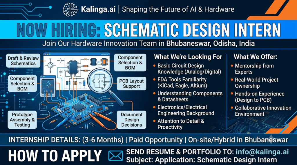
You’ll work with our engineering team on schematic capture, component selection, and PCB layout support for a new hardware product. You’ll get direct mentorship and real ownership of design tasks as the project moves from concept toward prototype.
Responsibilities
- Draft and review circuit schematics using EDA tools (KiCad, Eagle, Altium, or similar)
- Assist with component selection, datasheet review, and BOM preparation
- Support PCB layout, footprint creation, and design rule checks
- Help with prototype assembly, bring-up, and basic testing/debugging
- Document design decisions, revisions, and test results clearly
- Collaborate with firmware/embedded engineers on hardware-software interface points
Requirements
- Working knowledge of circuit design fundamentals (analog/digital electronics)
- Familiarity with schematic capture tools (KiCad, Eagle, Altium, OrCAD, or similar)
- Basic understanding of components: microcontrollers, power regulators, connectors, passives
- Currently pursuing or recently completed a degree in Electronics, Electrical Engineering, or related field
- Attention to detail and comfort reading datasheets
- Personal projects, coursework, or hackathon builds involving PCB design are a strong plus
Nice to Have
- Exposure to PCB layout and routing (not just schematic capture)
- Basic understanding of signal integrity, power distribution, or EMI/EMC basics
- Experience with 3D printing or rapid prototyping
- Familiarity with embedded systems or firmware (helps with hardware-software collaboration)
Details
- Duration: 6 months
- Stipend: Paid internship, details discussed during interview
- Mode: Hybrid
How to Apply
Send your resume, a short note on relevant schematic/PCB design projects you’ve worked on, and any portfolio links (GitHub, design files, or images of past boards) to:
Please use the subject line: “Application: Schematic Design Intern”