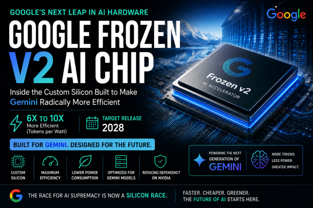
Google is developing a new in-house server chip, internally codenamed “Frozen v2,” designed to run its Gemini models far more efficiently than its current hardware. The chip is reportedly targeting a release around 2028 and could deliver between six and ten times the efficiency of Google’s existing AI accelerators, measured in tokens generated per unit of power.
That single fact — a potential 6x to 10x jump in tokens-per-watt — is why the story moved Alphabet’s stock and why every major AI lab is suddenly racing to build its own silicon. Here’s what the Google Frozen v2 AI chip actually is, why it matters, and how it fits into the broader arms race to escape Nvidia’s grip on AI computing.
What Is the Google Frozen v2 AI Chip?
The Google Frozen v2 AI chip is a next-generation custom accelerator that Alphabet is reportedly designing to power its Gemini AI models more efficiently in production. The project was first reported by The Information, which cited anonymous sources familiar with the effort. Google itself has not confirmed the chip by name, but it also hasn’t denied the report.
When TechCrunch asked Google directly about the project, the company offered a carefully worded non-denial:
Google said its teams are constantly experimenting with new hardware and software innovations, and that this exploration — while not every project reaches production — is central to its “full stack approach” of co-designing hardware and software together.
Definition + Expansion: In practical terms, this new chip is best understood as Google’s next attempt to close the gap between how much compute Gemini needs and how much power that compute actually consumes. Every additional token an AI model generates costs electricity, cooling, and data center capacity. A processor that generates the same number of tokens using a sixth to a tenth of the power fundamentally changes the economics of running a large language model at global scale.
Key Facts About the Frozen v2 AI Chip
- Codename: Frozen v2 (internal Google designation)
- Reported timeline: Expected release around 2028
- Efficiency target: 6x to 10x more efficient than Google’s current AI chips, measured in tokens per unit of power
- Purpose: Run Gemini models more cost-effectively at inference and training scale
- Source of the report: The Information, citing anonymous sources
- Google’s public stance: Neither confirmed nor denied
Why Google Is Building This Chip Now
The Efficiency Imperative
AI efficiency has quietly become the most important metric in the industry, arguably more important than raw model capability. As AI companies scale up data centers that draw hundreds of megawatts, the chip that delivers the most useful output per watt is the one that wins deployment at scale — not necessarily the chip with the highest peak performance on paper.
This shift matters because power, not chip count, is increasingly the bottleneck. Grid interconnect timelines, cooling infrastructure, and electricity availability are gating how fast hyperscalers like Google can expand their AI footprint through the rest of the decade. A more efficient successor to today’s TPUs would let Google serve more Gemini traffic without needing a proportional increase in power capacity — a critical advantage when new data center power is scarce and expensive to build.
Google’s existing Tensor Processing Units already reflect this efficiency-first design philosophy. The seventh-generation TPU, Ironwood, delivered roughly double the performance per watt of its predecessor and was positioned specifically for inference workloads rather than training. Frozen v2 appears to be the next major leap in that same lineage, pushing efficiency gains far beyond incremental generational improvements.
Breaking Free From Nvidia
Question: Why are AI companies building their own chips instead of just buying more Nvidia GPUs?
Direct Answer: Because relying entirely on one supplier is both expensive and risky. Nvidia has historically dominated the AI chip market, and that dominance has left major AI labs dependent on its hardware, its pricing, and its supply constraints. Building custom silicon lets Google control its own hardware roadmap, tune chips specifically for its own models, and reduce exposure to Nvidia’s pricing power and allocation decisions.
This is not a Google-only strategy. Every major AI lab is now pursuing custom silicon:
- OpenAI unveiled its first custom chip, an inference processor codenamed Jalapeño, built in partnership with Broadcom.
- Anthropic has reportedly been in talks with Samsung about a new custom chipmaking partnership.
- Google is now reportedly working on Frozen v2 as a successor to its TPU line, specifically to make Gemini more efficient.
The pattern is consistent: as AI spending faces increased scrutiny from investors, efficiency and hardware independence have become competitive necessities rather than side projects.
From TPU v2 to Frozen v2: Google’s Custom Silicon Journey
Google has been building its own AI chips longer than almost anyone else in the industry, and that history helps explain why a 6x-to-10x efficiency claim is plausible rather than pure marketing. Google’s Tensor Processing Units have gone through seven public generations, and each one has prioritized performance-per-watt alongside raw throughput:
- TPU v4 delivered roughly 2.7x better performance per watt than TPU v3, driven largely by improved interconnects and denser compute.
- Trillium, the sixth-generation TPU, improved efficiency by around 67% over its predecessor, TPU v5e.
- Ironwood, the current seventh-generation TPU, doubled performance-per-watt again relative to Trillium, while also expanding memory bandwidth and capacity to support larger, more complex models.
Each generation has compounded on the last, and Google has said its versatile TPU cohort is now roughly 30 times more efficient than its very first Cloud TPU from 2018. Viewed against that backdrop, this new project isn’t a sudden departure from Google’s strategy — it’s the next data point in a decade-long trend of squeezing more useful computation out of every watt of power. What makes it notable is the size of the projected jump and its explicit framing around Gemini specifically, rather than TPUs as general-purpose cloud infrastructure.
How Efficient Will the Frozen v2 AI Chip Be?
The headline number — a possible 6x to 10x efficiency gain over Google’s current AI chips — is measured in tokens generated per unit of power. That’s a meaningfully different, and arguably more useful, metric than raw compute throughput, because it captures what actually matters for running a chatbot or AI agent at scale: how many useful responses a data center can generate per dollar of electricity.
To put that number in context, it helps to compare it against how Google’s existing TPU line has progressed generation over generation:
| Chip Generation | Reported Performance-per-Watt Gain | Primary Focus |
|---|---|---|
| TPU v4 | ~2.7x better than TPU v3 | Training |
| Trillium (6th gen TPU) | ~67% improvement over TPU v5e | Training & inference |
| Ironwood (7th gen TPU) | ~2x better than Trillium | Inference at scale |
| Frozen v2 (reported) | 6x–10x better than current chips | Gemini efficiency |
Definition + Expansion: If accurate, a 6x to 10x jump would represent a far larger single-generation leap than anything Google has achieved with its TPU line to date, where efficiency gains have typically landed in the 2x range per generation. That’s precisely why the report was significant enough to move Alphabet’s stock — it suggests either a genuine architectural breakthrough or a longer development runway (the chip isn’t expected until 2028) that allows for more aggressive engineering targets than a typical one-to-two-year TPU refresh cycle.
It’s also worth noting that efficiency in AI chip design isn’t just about the processor itself. Google’s recent TPU generations have paired chip-level gains with system-level improvements — liquid cooling, optical interconnects, and data center power usage effectiveness — that compound the final efficiency number. Frozen v2 will likely benefit from the same full-stack approach Google described in its statement to TechCrunch.
Google Frozen v2 AI Chip vs. Rivals: How the Custom Chip Race Compares
Google isn’t alone in building efficiency-focused custom silicon. Here’s how the major reported efforts compare:
| Company | Custom Chip | Manufacturing Partner | Stated Goal | Reported Timeline |
|---|---|---|---|---|
| Frozen v2 | Not disclosed | 6x–10x efficiency gain for Gemini | ~2028 | |
| OpenAI | Jalapeño | Broadcom | Efficient in-house inference | Announced June 2026 |
| Anthropic | Unnamed (in talks) | Samsung (reported) | Reduce Nvidia dependence | Talks reported July 2026 |
| Google (current) | Ironwood (TPU v7) | Broadcom | 2x efficiency vs. Trillium | Available now |
This table highlights a clear industry pattern: efficiency-per-watt, not raw compute power, has become the central battleground for custom AI silicon. Every lab racing to build its own chip is chasing the same underlying goal — generating more usable AI output per unit of electricity, at lower cost, with less dependence on Nvidia.
What This Means for Google’s AI Strategy and Gemini
The Capital Expenditure Context
Google’s AI ambitions come with an enormous price tag. Earlier this year, the company said it plans to spend between $180 billion and $190 billion on its AI buildout. Investors have previously voiced concern about the scale of that spending relative to near-term returns, especially as broader anxiety about AI capital expenditure has cooled market enthusiasm across the tech sector.
Against that backdrop, a new chip promising a 6x to 10x efficiency improvement functions as a direct answer to investor skepticism. If Google can generate significantly more AI output per dollar of infrastructure spend, its enormous capex commitments look far more defensible, since every dollar spent on data centers and power stretches further.
The Market Reaction
The market response to the report was immediate. Following the initial story, Alphabet’s stock climbed roughly 3% in a single trading session, arriving just ahead of the company’s next earnings report. That reaction reflects how central hardware efficiency has become to how Wall Street values AI companies — not just what models they build, but how cheaply and sustainably they can run them.
What It Means for Gemini Specifically
For everyday users and enterprise customers, a more efficient underlying chip doesn’t change what Gemini can do overnight — 2028 is still years away. But over time, it typically translates into:
- Lower inference costs, which can mean cheaper API pricing or more generous free-tier usage for Gemini
- Faster response times, since more efficient chips can process more tokens per second within the same power envelope
- Greater deployment scale, allowing Google to serve more Gemini traffic without being constrained by data center power limits
- More competitive positioning against OpenAI’s Jalapeño-powered infrastructure and Anthropic’s Samsung-built silicon
Timeline: When Will the Frozen v2 AI Chip Launch?
Question: When will Google’s new chip actually be available?
Direct Answer: According to the initial report, the Frozen v2 AI chip is slated for release sometime in 2028 — meaning it’s still in an early development phase and years away from powering production Gemini traffic.
That timeline matters for two reasons. First, it explains why the projected efficiency gains are so aggressive: a longer development cycle allows for more ambitious architectural changes than an annual refresh would. Second, it means Frozen v2 won’t be Google’s only efficiency lever between now and 2028 — expect continued TPU generations, successors to Ironwood, to arrive in the interim, incrementally improving performance-per-watt while the newer chip is finalized.
What Analysts Are Watching Next
With the chip still roughly two years from any confirmed launch, most of the near-term signal will come from indirect sources rather than an official Google product announcement. Analysts covering Alphabet are likely to watch a few specific indicators over the coming quarters:
- Google’s earnings commentary on infrastructure efficiency and capital expenditure discipline, especially given the company’s $180–190 billion AI buildout plan
- Any successor TPU announcements at future Google Cloud Next events, which could reveal whether efficiency gains are tracking toward the reported 6x–10x target
- Hiring and supply chain signals, such as new fabrication partnerships, that might confirm which manufacturer is producing the chip
- Competitive responses from Nvidia, OpenAI, and Anthropic, whose own chip roadmaps will shape how urgently Google needs to hit its efficiency targets
Because Google neither confirmed nor denied the report, expect the company to stay largely quiet on specifics until it’s ready to make a formal announcement, likely tied to a future Google Cloud Next keynote or a Gemini infrastructure update. In the meantime, the reaction from investors already shows how much weight the market is putting on efficiency as the defining metric of the next phase of the AI buildout — arguably more than any single new model release.
Frequently Asked Questions
Is the Frozen v2 AI chip confirmed by Google? Not officially. Google has not confirmed the chip by name and has neither denied nor validated the specific details reported by The Information. Its public statement acknowledged ongoing hardware experimentation without confirming this specific project.
How is the Frozen v2 AI chip different from Google’s TPUs? Google’s TPUs are its existing line of custom AI accelerators, now in their seventh generation with Ironwood. Frozen v2 appears to be positioned as a future, more efficiency-focused successor within that broader custom silicon strategy, though Google hasn’t clarified its exact relationship to the TPU naming convention.
Why does chip efficiency matter more than raw processing power? Because power availability, not raw compute, is increasingly the limiting factor for scaling AI. A chip that produces more tokens per watt lets a company serve more users and run larger models without needing proportionally more electricity and data center capacity, both of which are expensive and slow to build.
How does the Frozen v2 AI chip compare to OpenAI’s and Anthropic’s chip efforts? All three efforts share the same underlying motivation: reducing dependence on Nvidia and improving efficiency for in-house models. OpenAI’s Jalapeño chip, built with Broadcom, is already announced and focused on inference. Anthropic’s reported talks with Samsung are still in early stages. Google’s project has the most aggressive stated efficiency target but also the longest reported timeline, at around 2028.
Will the Frozen v2 AI chip lower the price of using Gemini? It’s too early to say with certainty, but historically, efficiency gains in Google’s TPU line have translated into lower cloud compute pricing and better price-performance for customers over time. A 6x-to-10x efficiency jump, if realized, would give Google significant room to make Gemini more competitively priced against rivals.
The Bottom Line
The Google Frozen v2 AI chip represents a significant escalation in the industry-wide push toward custom, efficiency-first AI silicon. Whether or not the 6x-to-10x efficiency claim holds up by the time the chip actually ships in 2028, the report itself signals where the entire AI industry is heading: away from generic GPU dependence and toward vertically integrated hardware built specifically to make each company’s own models run leaner, cheaper, and faster. For Google, this project isn’t just an engineering exercise — it’s a direct response to investor pressure to prove that its massive AI infrastructure spending will eventually pay for itself.
Meta Description: Google is reportedly building a new AI chip, Frozen v2, aiming for 6x–10x better efficiency to power Gemini models more cost-effectively by 2028.
Slug: google-frozen-v2-ai-chip